Single particle surface plasmon electrooptical modulator and manufacturing method thereof

A surface plasmon, electro-optic modulator technology, applied in instruments, optics, nonlinear optics, etc., can solve problems such as unfavorable device miniaturization and speed improvement, and achieve small device size, high response rate, and response speed. quick effect

Active Publication Date: 2018-01-19
PEKING UNIV
View PDF2 Cites 14 Cited by
  • Summary
  • Abstract
  • Description
  • Claims
  • Application Information

AI Technical Summary

Problems solved by technology

Traditional electro-optic modulation devices are all on the order of microns, which is not conducive to the miniaturization of devices and the improvement of speed

Method used


Image

  • Single particle surface plasmon electrooptical modulator and manufacturing method thereof
  • Single particle surface plasmon electrooptical modulator and manufacturing method thereof
  • Single particle surface plasmon electrooptical modulator and manufacturing method thereof

Examples


preparation example Construction

[0053] The preparation method of the molybdenum disulfide-based single-particle surface plasmon electro-optic modulator is further given below, and the preparation of the electro-optic modulator includes the following steps:

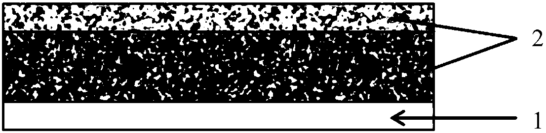
[0054] Step 1, the SiO 2 / Si substrate is ultrasonically cleaned with an organic solvent, and ultrasonically cleaned in the order of acetone (10-15min)→ethanol (10-20min)→deionized water (20-30min), and finally the remaining on the substrate is cleaned with a nitrogen gun. Blow dry with deionized water to get clean SiO 2 / Si substrate.

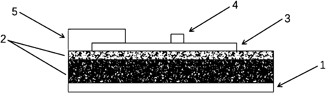
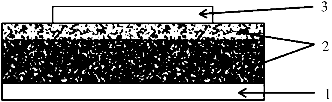
[0055] Step two, such as figure 2 As shown, the SiO obtained in the previous step 2 The Si surface of the / Si substrate 2 is coated with Ti and Au as the bottom electrode 1 in turn by using electron beam evaporation coating method to obtain SiO with the bottom electrode. 2 / Si substrate. In order to obtain better film thickness and quality, the vacuum degree of the electron beam evaporation coating instrument shoul...

Embodiment 1

[0062] Optical diagram of a single-particle surface plasmon electro-optic modulator based on molybdenum disulfide Figure 6 As shown, from bottom to top including bottom electrode 1, SiO 2 / Si substrate 2, single-layer molybdenum disulfide 3, metal nanodisc 4 and top electrode 5. Among them, the bottom electrode 1 is in SiO 2 / Si substrate 2, the monolayer molybdenum disulfide 3 after wet transfer is in SiO 2 / Si substrate 2, the metal nano-disc 4 produced by electron beam exposure is on the single-layer molybdenum disulfide 3, the material of the metal nano-disc 4 is gold, the height is 30nm, and the radius is 60nm (under this size, The coupling efficiency calculated by FDTD solutions software is the best). The top electrode 5 is above the single layer of molybdenum disulfide 3 and away from the area of ​​the metal nanodisc 4 . Both the top electrode 5 and the bottom electrode 1 are obtained by evaporating 5nmTi / 80nm Au by electron beam evaporation coating. The two electro...


PUM

PropertyMeasurementUnit
thicknessaaaaaaaaaa
lengthaaaaaaaaaa
thicknessaaaaaaaaaa

Abstract

The invention discloses a single particle surface plasmon electrooptical modulator and a manufacturing method thereof. The electrooptical modulator realizes active modulation on scattering light intensity in a visible band. The electrooptical modulator comprises a bottom electrode, a conductive substrate, an insulating layer, and a monolayer transition metal chalcogenide. The monolayer transitionmetal chalcogenide has a metal nano structure and a top electrode which are far away from each other. The bottom electrode and the top electrode are connected with external modulating voltage, to forman anode and a cathode of the electrooptical modulator. The anode and the cathode are isolated by an insulating layer, to form a plate capacitor structure. When the external modulating voltage is applied, Fermi level of the transition metal chalcogenide moves to change optical properties of the transition metal chalcogenide, and coupling strength of the transition metal chalcogenide and the metalnano structure changes therewith, so that modulation on a scattered optical field is realized. The electrooptical modulator is the first electrooptical modulator which realizes optical field modulation on a nanoscale, and the electrooptical modulator operates in a visible band, and is characterized by high stability and fast response speed.

Description

technical field [0001] The invention relates to a novel electro-optic modulator, in particular to a single-particle surface plasmon electro-optic modulator based on a transition metal chalcogenide, which can realize electrical modulation of optical signals on a nanometer scale. Background technique [0002] In the field of nanotechnology, the most important thing to realize high-speed optoelectronic devices is to realize the regulation of light in the integrated circuit on chip. Traditional electro-optic modulation devices are all on the order of microns, which is not conducive to the miniaturization of devices and the improvement of speed. Therefore, the realization of nanoscale electro-optic modulators has become an urgent problem to be solved. [0003] In recent years, transition metal chalcogenides represented by molybdenum disulfide and tungsten disulfide have shown various electronic properties. Compared with traditional three-dimensional optical materials, two-dimen...

Claims


Application Information

Patent Timeline
Patent Type & Authority Applications(China)
IPC IPC(8): G02F1/015G02F1/03
Inventor 方哲宇李博文朱星祖帅蒋瞧
Owner PEKING UNIV
Why Eureka
Try Eureka