Intercalation molybdenum oxide single crystal film as well as preparation method and purpose thereof

A technology of molybdenum oxide and molybdenum trioxide, applied in chemical instruments and methods, single crystal growth, single crystal growth, etc., can solve problems such as oxygen vacancy defects, material failure, and device response time increased to tens to hundreds of seconds , to achieve the effect of improving conductivity, expanding the interband state, and broadening the photoresponse range

Active Publication Date: 2018-02-06
JINAN UNIVERSITY
View PDF3 Cites 7 Cited by
  • Summary
  • Abstract
  • Description
  • Claims
  • Application Information

AI Technical Summary

Problems solved by technology

[0005] However, the above methods all destroy the lattice structure of the material, resulting in oxygen vacancy defects
The generation of oxygen vacancy defects leads to the material's response to H 2 O, O 2 Sensitive, so the light, heat and atmosphere stability of the device are greatly reduced, and it cannot work stably in the atmospheric environment
Although the device can work in a vacuum environment, the appearance of oxygen vacancies in a vacuum environment also leads to a significant increase in the response time of the device to the order of tens to hundreds of seconds.
Finally, small ions such as implanted H and Li have high mobility in the oxide, and can move under the action of an electric field, resulting in the precipitation of ions and the rapid failure of the material.
Therefore, the existing methods cannot achieve the broadening of the material response band, the improvement of device stability and the improvement of response speed at the same time.

Method used


Image

  • Intercalation molybdenum oxide single crystal film as well as preparation method and purpose thereof
  • Intercalation molybdenum oxide single crystal film as well as preparation method and purpose thereof
  • Intercalation molybdenum oxide single crystal film as well as preparation method and purpose thereof

Examples


Embodiment 1

[0037] The preparation of the intercalated molybdenum oxide nanomaterial and its application in photodetectors comprises the following steps:

[0038] (1) Preparation of MoO 3 Single wafer: take 1 g of molybdenum trioxide powder (purity 99.9%) and place it in a square ceramic crucible with a length of 5 cm and a width of 2 cm. Place the crucible in a tube furnace, with both ends closed if not completely sealed, and the knobs at both ends are opened to let air in and out, and the air humidity is ~40%. Heat the crucible to 780 °C for 1 h, and use a quartz substrate to obtain MoO in the low temperature region 3 single chip.

[0039] (2) Preparation of stannous oxide solution: successively add 0.1g SnCl 2 and 1g of L-tartaric acid were added to 50mL of deionized aqueous solution and ultrasonicated for 15min to obtain 10mM SnCl 2 solution.

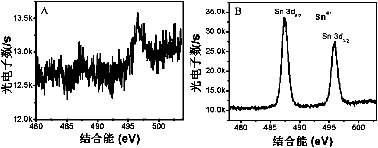
[0040] (3) Add 0.1g MoO 3The single wafer is immediately soaked in the stannous oxide solution, at this time the stannous oxide and MoO ...

Embodiment 2

[0049] The preparation of the intercalated molybdenum oxide nanomaterial and its application in photodetectors comprises the following steps:

[0050] Steps (1)-(4) are the same as in Example 1;

[0051] (5) Use a dropper to drop the intercalation molybdenum oxide single wafer suspension to 500nm thick SiO 2 On the Si wafer substrate, the dispersed doped molybdenum oxide single wafer can be obtained after natural air drying;

[0052] (6) Pass the doped molybdenum oxide single wafer through a microscopic mask, thermally evaporate a 1nm thick LiF film as an electron transport layer, and then plate a 100nm thick metal Au electrode to construct a single single wafer resistive photodetector device.

[0053] The experimental results of the response of the prepared device to the laser wavelengths of 405nm, 520nm and 638nm under the bias voltage of 0.3V and different powers are as follows: Figure 9 As shown, the results show that the prepared devices have responses at 405nm, 520nm ...


PUM


Abstract

The invention discloses an intercalation molybdenum oxide single crystal film as well as a preparation method and a purpose thereof. The method comprises the following steps of heating molybdenum trioxide powder to be 580 to 880 DEG C in atmospheric environment; maintaining the state for not less than 1 hour; then, cooling the materials to 350 to 550 DEG C; performing collection by a substrate toobtain a molybdenum oxide single crystal sheet; dissolving SnCl2 into de-ionized water; adding the molybdenum oxide single crystal sheet; heating the reaction system to be 30 to 90 DEG C; performing reaction for 10 to 180 min; washing a product to obtain a suspension; treating the suspension by a suction filtration method or dispersing the suspension onto the required substrate to obtain the intercalation molybdenum oxide single crystal film. The ion intercalation method is used for intercalating Sn<4+> metal ions into MoO3 interlayer Van der Waals gaps; the between-band state is obviously expanded under the condition of avoiding the oxygen vacancy generation; the conductivity of the MoO3 is obviously improved; the light response range of the MoO3 is expanded, so that the response to ultraviolet light, visible light and near infrared light are realized.

Description

technical field [0001] The invention belongs to the field of semiconductor optoelectronic materials, and in particular relates to an intercalated molybdenum oxide single crystal film and its preparation method and application. Background technique [0002] The two-dimensional layered semiconductor molybdenum oxide material has a high dielectric constant and can effectively suppress the Coulomb scattering of carriers, so the material has a particularly high carrier mobility. In 2013, S Balendhran et al. measured the field-effect mobility of carriers in this type of material from the laboratory, and its value reached 1100cm 2 / Vs. In 2017, WB Zhang et al. further predicted layered MoO 3 The theoretical carrier mobility at room temperature can be as high as 3000 cm 2 / Vs, this value is at least an order of magnitude higher than common oxide materials, comparable to semiconductor Si materials. [0003] The two-dimensional molybdenum oxide material also has a band gap of >...

Claims


Application Information

Patent Timeline
Patent Type & Authority Applications(China)
IPC IPC(8): C30B29/16C30B29/64C30B29/68
CPCC30B29/16C30B29/64C30B29/68
Inventor 谢伟广何锐辉王雨
Owner JINAN UNIVERSITY
Why Eureka
Try Eureka