Sinterable bonding material and semiconductor device using the same
A technology of adhesive materials and silver fillers, which is applied in semiconductor devices, adhesive heating bonding methods, semiconductor/solid-state device manufacturing, etc., can solve problems such as peeling off of bonded parts and cracks, and achieve excellent long-term reliability Effect
- Summary
- Abstract
- Description
- Claims
- Application Information
AI Technical Summary
Problems solved by technology
Method used
Image
Examples
preparation example Construction
[0059] Examples of the preparation method of the silver filler whose surface is coated with an organic substance include, but are not limited to, a method of preparing the silver filler by a reduction method in the presence of an organic solvent. Specifically, for example, the silver filler can be obtained by mixing a silver carboxylate salt with a primary amine, and depositing the silver filler using a reducing agent in the presence of an organic solvent, as described in Japanese Patent Laid-Open Nos. 2006-183072 and 2011-153362, etc. . In addition, the silver filler can be obtained by the method described in Japanese Patent Laid-Open No. 2014-196527, which includes the step of dispersing silver oxalate using a carrier medium such as water or alcohol and a dispersion medium such as glycols, followed by applying heat and / or stress. The foregoing applications are hereby incorporated by reference in their entireties.
[0060] It is also preferred to disperse the obtained silve...
Embodiment 1
[0202]
[0203] Silver fillers, resin particles, additives, and solvents were mixed in the proportions shown in Table 1 to prepare an adhesive material.
[0204]
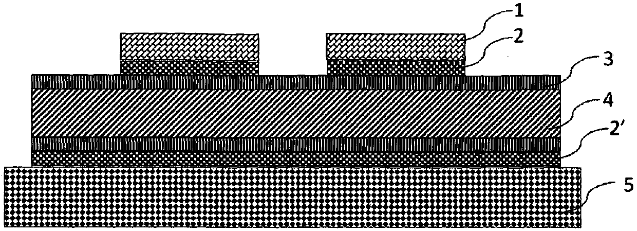
[0205] The obtained adhesive material was printed on a substrate (silver-plated copper lead frame, 25×25 mm, thickness 0.3 mm) at a thickness of 100 μm. A semiconductor chip (silver-plated backside Si die, 10×10 mm) was mounted on the substrate. The substrate with the chip was dried at 90° C. for 30 minutes, and heated in an oven under the conditions of 300° C. / 5 minutes / 10 MPa to obtain a sample for evaluation. The thickness of the bonding layer after sintering is about 40 to 60 μm.
[0206] Warpage generated during sintering was measured using a three-dimensional length measuring machine (KS-1100, manufactured by Keyence Corporation).
[0207]
[0208] The obtained adhesive material was printed at a thickness of 100 μm between two substrates (500 μm thick, silver-plated copper of 5 mmΦ). The two substrate...
PUM
| Property | Measurement | Unit |
|---|---|---|
| roughness | aaaaa | aaaaa |
| tensile modulus | aaaaa | aaaaa |
| thermal degradation temperature | aaaaa | aaaaa |
Abstract
Description
Claims
Application Information


