Novel electromagnetic wave absorption material and preparation method thereof

A technology of absorbing materials and absorbing composite materials, applied in the field of electromagnetic wave absorbing materials, can solve the problems of difficult to reach working frequency, low absorption rate, small bandwidth range, etc. Effect

Active Publication Date: 2018-03-06
PEKING UNIV
View PDF4 Cites 1 Cited by
  • Summary
  • Abstract
  • Description
  • Claims
  • Application Information

AI Technical Summary

Problems solved by technology

"Broadband and thin microwave absorber of nickel-zinc ferrite/carbonyl iron" (Journal of Alloys and Compounds 487 (2009) 708-711) discloses the wave-absorbing composite material of ferrite and metal particles; "Dependence of Microwave Absorbing Property on Ferrite Volume Fraction in MnZn Ferrite-Rubber Composites" (D.Y.Kim, Y.C.Chung, T.W.Kang, and H.C.Kim IEEETRANSACTIONSONMAGNETICS, VOL 32, NO 2, MARCH 1996) discloses the electromagnetic wave absorbing material of ferrite; and the frequency band of ferrite material is narrow, The density is high, the absorption rate is low, and its working frequency is generally difficult to reach the microwave band in the range of ultra-high frequency, ultra-high freq

Method used


Image

  • Novel electromagnetic wave absorption material and preparation method thereof
  • Novel electromagnetic wave absorption material and preparation method thereof
  • Novel electromagnetic wave absorption material and preparation method thereof

Examples


Embodiment 1

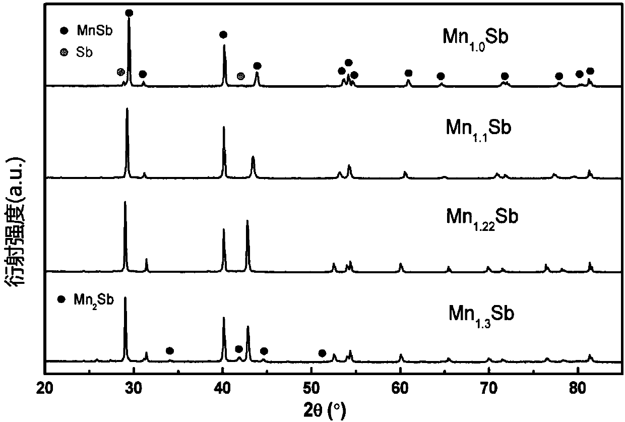
[0028] Weigh an appropriate proportion of manganese and antimony (atomic ratio Mn:Sb=x:1), prepare a master alloy by smelting, or rapidly solidify into alloy strips (1-2cm wide, 0.2-0.4mm thick) by smelting, and then Break into 50-100 micron coarse powder, and measure its diffraction spectrum by X-ray diffractometer. figure 1 for different Mn x In the XRD pattern of the Sb alloy, the main phase of the alloy shows a NiAs hexagonal structure, where the values ​​of x are 1.0, 1.1, 1.22, and 1.3, respectively.

Embodiment 2

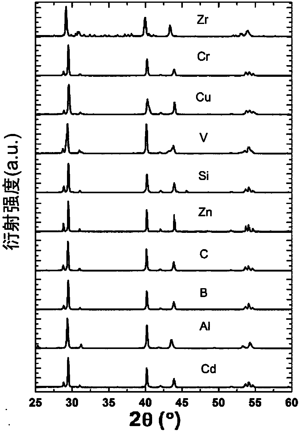
[0030] Weigh an appropriate proportion of manganese, antimony and the third element T (atomic ratio Mn:T:Sb=0.9:0.1:1), prepare a master alloy by smelting, or rapidly solidify into an alloy strip (1-2cm wide, 0.2-0.4mm thick), and then crushed into 50-100 micron coarse powder, the X-ray diffractometer was used to measure its diffraction spectrum. figure 2 Mn for adding different T elements 0.9 T 0.1 In the XRD pattern of Sb alloy, the main phase of the alloy is NiAs hexagonal structure, where T is Zr, Cr, Cu, V, Si, Zn, C, B, Al, Cd respectively. The effect of adding the third element T is to improve the stability of the material, improve the magnetization and Curie temperature of the material, and obtain excellent wave-absorbing characteristics.

Embodiment 3

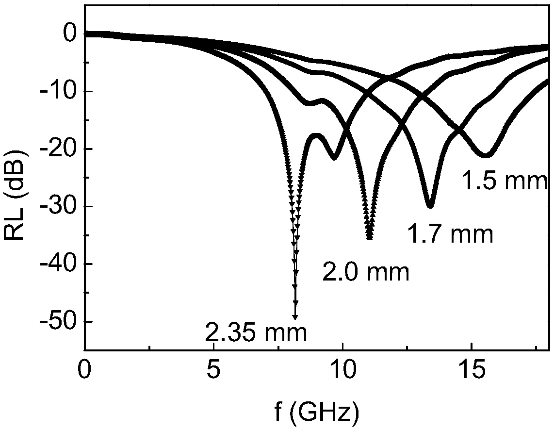
[0032] Weigh 73g of Mn and 147g of Sb, rapidly solidify into alloy ingots or alloy strips by smelting, then mechanically crush into 50-100 micron coarse powder, and ball mill the powder in gasoline and grinding aid solution for 15 hours. Drain the liquid after the ball mill is discharged, dry the magnetic powder, and make a composite bonded compression mold with paraffin wax (cylindrical ring with an inner diameter of 3.04 mm and an outer diameter of 7.00 mm). Electromagnetic properties were measured on an Agilent vector network analyzer. According to the measured electromagnetic parameters, it can be known by calculation that the absorption peak intensity of the material within the matching thickness range of 1.4-2.35mm exceeds -20dB, and the bandwidth less than -10dB is as high as 5.3GHz. The absorption strength reaches -50dB when the frequency is 8.2GHz (matching thickness is only 2.35mm). Absorption curve such as image 3 shown.


PUM

PropertyMeasurementUnit
The inside diameter ofaaaaaaaaaa
Outer diameteraaaaaaaaaa
Absorption strengthaaaaaaaaaa

Abstract

The invention discloses a novel electromagnetic wave absorption material and a preparation method thereof. The electromagnetic wave absorption material is an Mn-Sb alloy compound, and the general chemical formula is MnxSb or (Mn, T)xSb, wherein x is larger than 0.8 and is smaller than 1.4, and T is one or an arbitrary combination of Zr, Cr, Cu, V, Si, Zn, C, B, Al and Cd. The preparation method ofthe material comprises the steps of carrying out mixed smelting or rapid-setting ingot casting on Mn and Sb elements of which the atomic proportion of Mn to Sb or (Mn, T) to Sb is 0.8 to 1.4, so as to obtain an alloy of an NiAs hexagonal structure; and then, crushing the alloy into submicron particles capable of being utilized as an electromagnetic wave absorbent. The novel electromagnetic wave absorption material has an excellent absorption capacity for electromagnetic waves of which the frequency band is from 1 G to 100 G, the absorption capacity is high, and the working frequency band is wide; and besides, the frequency band position can be adjusted according to the utilization condition, and the electromagnetic wave absorption requirement in civil and military fields can be effectively met.

Description

technical field [0001] The invention relates to an electromagnetic wave absorbing material, especially an electromagnetic wave absorbing material specially suitable for working in a high-frequency and wide-band environment higher than 1G Hz frequency band after using Mn-based materials to control the ratio of Mn elements to precisely modulate material properties. Background technique [0002] In recent years, with the rapid development of information technology, continuous improvement of information transmission rate and processing frequency has become the goal that people continue to pursue. The widely used 2G mobile phones with a working frequency of 0.9-1.8GHz have been transformed into 3G mobile phones with a working frequency of 1.8-2.4GHz. Mobile phones, and soon developed into 4G mobile phones with a working frequency of around 3.5GHz. In addition, due to the improvement of computer computing speed, the clock frequency approaches 2GHz, and its transmission line actual...

Claims


Application Information

Patent Timeline
IPC IPC(8): C22C28/00C22C1/02C22C1/04H05K9/00G12B17/02
CPCH05K9/00G12B17/02C22C1/02C22C28/00C22C1/047
Inventor 杨金波刘顺荃王常生韩景智
Owner PEKING UNIV
Why Eureka
Try Eureka