Preparation method of organic light-emitting display panel

An electroluminescence display and display panel technology, applied in circuits, electrical components, electrical solid devices, etc., can solve the problems of low luminous efficiency, low hole injection rate, and insufficient luminous brightness.

Active Publication Date: 2018-05-08
WGTECH JIANGXI
View PDF3 Cites 2 Cited by
  • Summary
  • Abstract
  • Description
  • Claims
  • Application Information

AI Technical Summary

Problems solved by technology

[0004] Based on this, it is necessary to provide a method for preparing an organic electroluminescent display panel in view

Method used


Image

  • Preparation method of organic light-emitting display panel

Examples


preparation example Construction

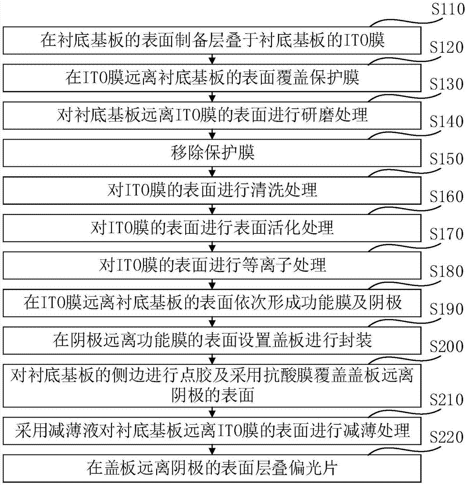
[0039] see figure 1 , the preparation method of the organic electroluminescence display panel of one embodiment comprises the following steps:

[0040] S110, preparing an ITO film stacked on the base substrate on the surface of the base substrate.

[0041] In one embodiment, the matrix frame is prepared on the base substrate first, and then an ITO film is formed on the base substrate by magnetron sputtering as an anode.

[0042] In one embodiment, the thickness of the formed ITO film is 300nm-350nm.

[0043] S120, covering the surface of the ITO film with a protective film.

[0044]In one embodiment, the step of covering the surface of the ITO film with a protective film specifically includes: coating the protective slurry on the ITO film to form a protective film.

[0045] Wherein, the protective slurry is prepared through the following steps:

[0046] In parts by mass, dissolve 9.5 to 9.9 parts of sodium hydroxide in 44.2 to 47.9 parts of water, and add 21.4 to 22.5 part...

Embodiment 1

[0095] Form an ITO film with a thickness of 300nm on the base substrate as an anode, cover the surface of the ITO film away from the base substrate with a protective film, and then grind the surface of the base substrate away from the ITO until the thickness of the base substrate is less than 0.5mm Remove the bumps and scratches on the surface of the substrate, and then remove the protective film on the surface of the ITO film.

[0096] The surface of the ITO film away from the substrate is cleaned with detergent solution, ethanol, acetone and water in sequence by spraying. After the cleaning is completed, the surface of the ITO film away from the substrate is treated with a surface treatment solution. For activation treatment, the surface treatment liquid includes a mixed solution of water, hydrogen peroxide and ammonia water, and the mass percentage of hydrogen peroxide is 15%, and the mass percentage of ammonia water is 15%. Then plasma treatment is performed on the surface...

Embodiment 2

[0100] Form an ITO film with a thickness of 350nm on the base substrate as an anode, cover the surface of the ITO film away from the base substrate with a protective film, and then grind the surface of the base substrate away from the ITO until the thickness of the base substrate is less than 1.0mm Remove the bumps and scratches on the surface of the substrate, and then remove the protective film on the surface of the ITO film.

[0101] The surface of the ITO film away from the substrate is cleaned with detergent solution, ethanol, acetone and water in sequence by spraying. After the cleaning is completed, the surface of the ITO film away from the substrate is treated with a surface treatment solution. For activation treatment, the surface treatment liquid includes a mixed solution of water, hydrogen peroxide and ammonia water, and the mass percentage of hydrogen peroxide is 13%, and the mass percentage of ammonia water is 13%. Then plasma treatment is performed on the surface...


PUM

PropertyMeasurementUnit
Work functionaaaaaaaaaa
Thicknessaaaaaaaaaa
Thicknessaaaaaaaaaa

Abstract

The invention relates to a preparation method of an organic light-emitting display panel. The preparation method of the organic light-emitting display panel comprises the following steps of preparingan ITO film stacked on a substrate on the surface of the substrate; carrying out cleaning treatment on the surface of the ITO film; carrying out surface activation treatment on the surface of the ITOfilm; carrying out plasma treatment on the surface of the ITO film until a work function of the surface of the ITO film is 5.2-5.6eV; sequentially forming a functional film and a cathode on the surface of the ITO film, wherein the functional film comprises a hole injection layer; and arranging a cover plate on the surface, far away from the functional film, of the cathode for carrying out packaging. According to the preparation method of the organic light-emitting display panel, the potential-energy difference between ITO and the hole injection layer can be effectively reduced, hole injectionis facilitated, the work function of the surface of the ITO film can be improved and the smoothness of the surface of the ITO film can be improved, so that the light-emitting efficiency of the organiclight-emitting display panel is further improved and the working life of the organic light-emitting display panel is further prolonged.

Description

technical field [0001] The invention relates to the field of display technology, in particular to a method for preparing an organic electroluminescence display panel. Background technique [0002] The basic structure of an organic electroluminescent display panel (OLED) is a thin, transparent indium tin oxide (ITO) layer with semiconductor properties connected to the positive electrode, plus another metal cathode, wrapped into a sandwich structure. The whole structural layer includes: hole transport layer (HTL), light emitting layer (EL) and electron transport layer (ETL). When the power is supplied to an appropriate voltage, the positive holes and the negative charges will combine in the light-emitting layer to produce light, and the three primary colors of red, green and blue RGB will be produced according to their formulas to form the basic colors. [0003] At present, due to the advantages of active light emission, high contrast ratio, and fast response speed, OLEDs are...

Claims


Application Information

Patent Timeline
IPC IPC(8): H01L51/56H01L51/52H01L27/32
CPCH10K59/12H10K50/81H10K71/00
Inventor 易伟华张迅张伯伦周慧蓉
Owner WGTECH JIANGXI
Why Eureka
Try Eureka