Light-driven SiC/GaN-based semiconductor device and manufacturing process thereof

A light-driven, semiconductor technology, applied in semiconductor devices, electrical components, circuits, etc., can solve the problem of reducing the effective area of ​​light energy absorption and photo-generated current density, the groove of the device cannot reach the expected depth, and affecting the performance of light-driven power devices. and other problems, to achieve the effect of reducing the surface breakdown electric field, reducing the cost of device application, and solving the weak anti-interference ability of EMI.

Pending Publication Date: 2018-05-15
UNIV OF ELECTRONIC SCI & TECH OF CHINA
View PDF0 Cites 2 Cited by
  • Summary
  • Abstract
  • Description
  • Claims
  • Application Information

AI Technical Summary

Problems solved by technology

However, since the transmission surface of UV light is not on the same plane, this greatly reduces the effective area of ​​light energy absorption and the photogenerated current density, which increases the required power for light triggering. In addition, because the current gain mechanism inside the device benefits from photogener

Method used


Image

  • Light-driven SiC/GaN-based semiconductor device and manufacturing process thereof
  • Light-driven SiC/GaN-based semiconductor device and manufacturing process thereof
  • Light-driven SiC/GaN-based semiconductor device and manufacturing process thereof

Examples


Example Embodiment

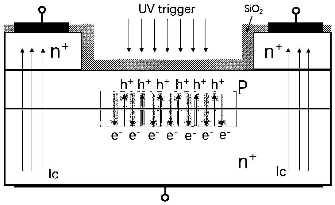
[0056] Example 1 An optically driven SiC-based semiconductor device

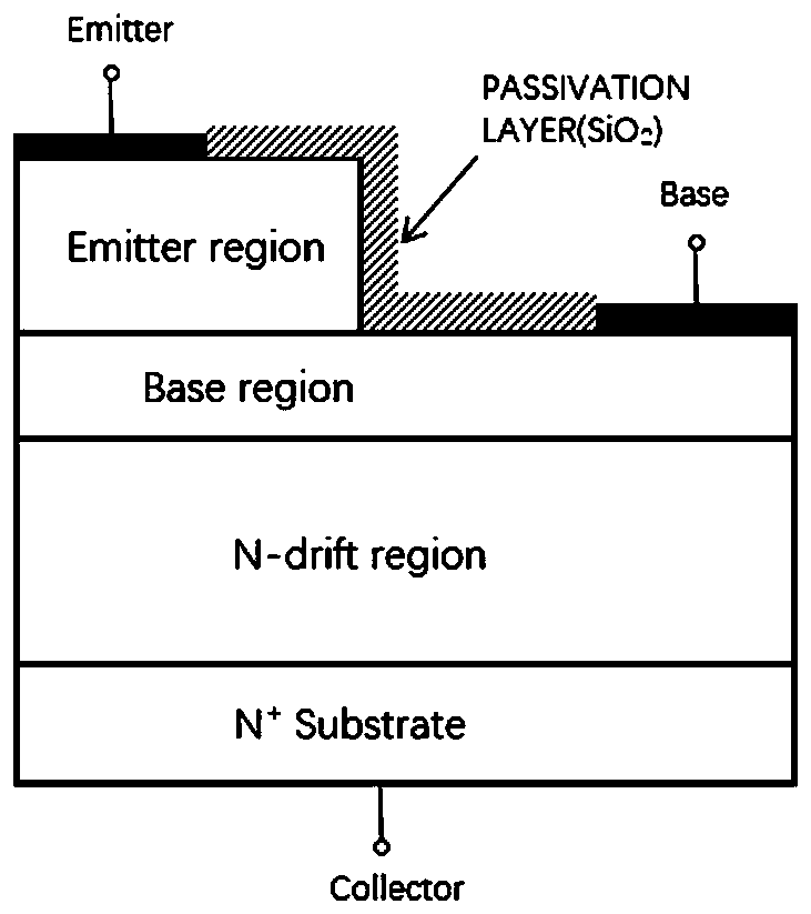
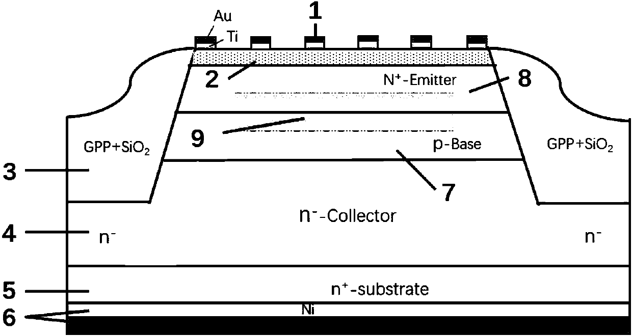
[0057] This embodiment provides a light-driven SiC-based semiconductor device, such as Figure 3-Figure 5 As shown, it includes an emitter structure, a P-type base region 7, a collector structure with an n-type collector region 4, an n+ type substrate structure, and a PN junction passivation protective layer arranged sequentially from top to bottom Structure 3; where

[0058] ①Emitter structure

[0059] The emitter structure includes a comb-shaped metal multilayer electrode 1, a transparent electrode 2 and an n+-type emitter region 8 arranged sequentially from top to bottom. The comb-shaped metal multilayer electrode 1 is located on the surface of the transparent electrode 2 and is in direct contact with the surface , The transparent electrode 2 forms an ohmic contact with the n+ type emitter region 8;

[0060] The comb-shaped metal multilayer electrode 1 is composed of a comb-shaped structure formed by multiple su...

Example Embodiment

[0076] Example 2 An optically driven GaN-based semiconductor device

[0077] The difference between this embodiment and embodiment 1 is:

[0078] In this embodiment, an n-type GaN wafer with a thickness of 300 μm is used as the substrate, the doping element selected for the p-type base region 7 is magnesium, and the n+ type emitter region 8, the n- type collector region 4 and the n+ type substrate 5 are selected The doping element is silicon.

[0079] The structure of the other parts of this embodiment is the same as that of the first embodiment.

[0080] The working principle of this embodiment is the same as that of the first embodiment.

Example Embodiment

[0081] Embodiment 3 A manufacturing process of an optically driven SiC / GaN-based semiconductor device

[0082] This example is used to make examples 1 and 2, such as Figure 7 As shown, the process is simplified and improved on the basis of the traditional BJT process. The manufacturing process mainly includes the following steps in sequence:

[0083] (1) Choose a commercial 8°off-axis n-type 4H-SiC single crystal wafer with a thickness of 400μm or an n-type GaN wafer with a thickness of 300μm as the substrate, and complete the n-type collector 4 and p-type on the substrate in turn For the epitaxial growth of the base region 7, an ion implantation process is used to form an n+ type emitter region 8 to form an epitaxial wafer;

[0084] (2) An ultra-high vacuum DC magnetron sputtering system is used to deposit a layer of indium tin oxide (ITO) transparent conductive film with a thickness of 20 to 200 nm on the epitaxial wafer as the transparent electrode 2, and then undergo annealing t...


PUM

PropertyMeasurementUnit
Thicknessaaaaaaaaaa
Thicknessaaaaaaaaaa
Thicknessaaaaaaaaaa

Abstract

The invention discloses a light-driven SiC/GaN-based semiconductor device. The base electrode in the traditional BJT structure is cancelled, and ultraviolet light passes through a transparent electrode and a thin emitter region and enters a base region to introduce light excitation and generate electron-hole pairs in order to provide a base current for the base of the BJT. A rounded quadrangular frustum device structure is adopted, which improves the withstand voltage of the device. The invention further discloses a process for manufacturing the light-driven SiC/GaN-based semiconductor device.The device has the same advantages as the traditional BJT. Moreover, the light injection current gain, breakdown voltage, EMI immunity, switching speed and stability of the device are improved, the driving loss and the response time are reduced, and the manufacturing cost is reduced. The light-driven SiC/GaN-based semiconductor device and the manufacturing process are applicable to the field of low-power and high-power semiconductor power devices.

Description

Technical field [0001] The invention belongs to the technical field of semiconductor devices, in particular to an optically driven SiC / GaN-based semiconductor device and its manufacturing process. Background technique [0002] In electronic power application systems, power semiconductor devices are widely used. From alarm clocks, mobile phones, digital cameras, and computers used in daily life, to large electrical power conversion equipment such as airplanes, ships, and spacecraft, power semiconductor devices are used for electrical energy conversion, power control and processing, and energy management adjustments The core devices of the company occupy a pivotal position. For a long time, power semiconductor devices based on Si materials have occupied a dominant position in electronic power systems. However, due to the limitations of the material itself, the performance of semiconductor power devices based on silicon materials has approached its theoretical limit in many aspects...

Claims


Application Information

Patent Timeline
IPC IPC(8): H01L29/41H01L29/739
CPCH01L29/41H01L29/739
Inventor 徐开凯钱津超赵建明于奇刘继芝夏建新周伟
Owner UNIV OF ELECTRONIC SCI & TECH OF CHINA
Why Eureka
Try Eureka