Preparation method and application of silicon-based spiny nanocone ordered array

An ordered array and nanocone technology, applied in nanostructure manufacturing, nanotechnology, nanooptics, etc., can solve the problems of unsatisfactory Raman enhancement effect and low sensitivity, and achieve clean surface, high sensitivity and large structural area. Effect

Inactive Publication Date: 2018-05-18
HEFEI INSTITUTES OF PHYSICAL SCIENCE - CHINESE ACAD OF SCI
View PDF5 Cites 20 Cited by
  • Summary
  • Abstract
  • Description
  • Claims
  • Application Information

AI Technical Summary

Problems solved by technology

In the prior art, the silicon material produced by reactive ion etching technology is generally an ordered array of silicon-based single-thorn nanocones, but this single-thorn-structured sil

Method used


Image

  • Preparation method and application of silicon-based spiny nanocone ordered array
  • Preparation method and application of silicon-based spiny nanocone ordered array
  • Preparation method and application of silicon-based spiny nanocone ordered array

Examples


preparation example Construction

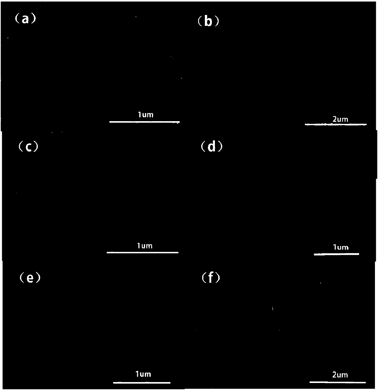
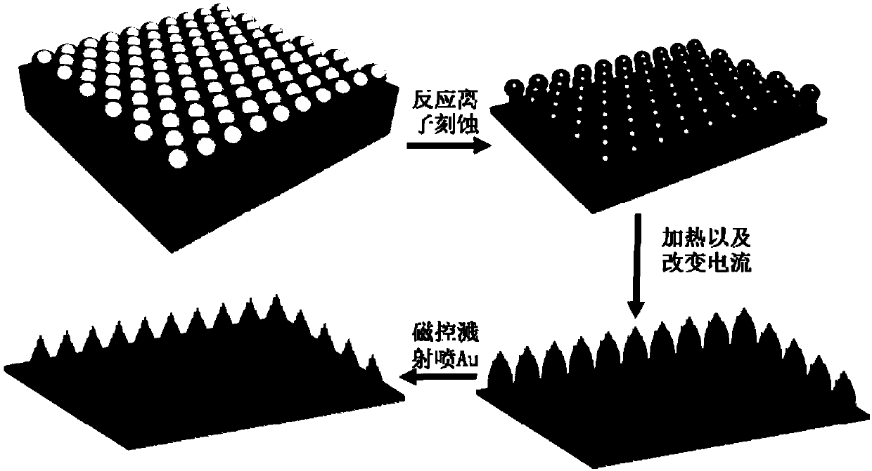
[0026] Such as image 3 Shown, a kind of preparation method of silicon-based spiny nanocone ordered array, comprises the steps:

[0027] Step A, preparing a single-layer ordered array of PS spheres (that is, polymer colloidal crystal spheres) closely arranged on the silicon wafer substrate, thereby obtaining a single-layer ordered array of PS spheres on the silicon wafer substrate.

[0028] Step B, heating the single-layer ordered PS ball array on the silicon wafer substrate, and then etching by reactive ion etching, and at least once increasing and adjusting the etching current during the etching process, and then After the etching is completed, the monolayer ordered PS sphere array on the silicon wafer substrate is removed, thereby preparing the silicon-based spiny nanocone ordered array.

Embodiment approach

[0030] (1) The described preparation of a tightly arranged single-layer ordered PS ball array on a silicon wafer substrate may include the following steps:

[0031] Step A1, put the silicon wafer base into acetone, ethanol, the first mixed solution, and deionized water in sequence for ultrasonic cleaning, then dry the cleaned silicon wafer base, and then place it in an ultraviolet ozone cleaner for 10 days of irradiation. ~40min to obtain a silicon wafer substrate with a hydrophilic surface. The first mixed solution is formed by mixing concentrated sulfuric acid with a mass concentration of 1.84 g / ml and hydrogen peroxide with a mass concentration of 1.1 g / ml in a volume ratio of 3:1.

[0032] Step A2, put the silicon chip substrate treated in step A1 into PS sphere ethanol diluent, and prepare a single-layer ordered PS in a hexagonal close-packed arrangement on the silicon chip substrate by using the gas-liquid interface self-assembly method. ball array. In practical applic...

Embodiment 1

[0046] Such as image 3 As shown, a method for preparing a silicon-based spiny nanocone ordered array may specifically include the following steps:

[0047] Step a1, put the silicon chip substrate into acetone, ethanol, and the first mixed solution in turn (the first mixed solution is composed of concentrated sulfuric acid with a mass concentration of 1.84g / ml and hydrogen peroxide with a mass concentration of 1.1g / ml according to the volume ratio of 3 :1 mixed), ultrasonically cleaned in deionized water, ultrasonically cleaned in each liquid for 30-40 minutes, and then dried on the cleaned silicon substrate, the drying temperature was 120°C, and the drying time was 20 minutes ; After the water on the silicon wafer is completely evaporated, the silicon wafer is placed in an ultraviolet ozone cleaning machine for 10-40 minutes of irradiation, thereby making a silicon wafer substrate with a hydrophilic surface.

[0048] Step b1: Take 50 microliters of PS sphere suspension (2.5 ...


PUM

PropertyMeasurementUnit
Diameteraaaaaaaaaa
Thicknessaaaaaaaaaa
Thicknessaaaaaaaaaa

Abstract

The invention discloses a preparation method and application of a silicon-based spiny nanocone ordered array. The preparation method comprises the steps: preparing a tightly-arranged single-layer ordered PS sphere array on a silicon wafer substrate; heating the single-layer ordered PS sphere array on the silicon wafer substrate; then, carrying out etching by using a reactive ion etching method, and regulating an etching current at least once in the etching process; and then, after finishing the etching, removing the single-layer ordered PS sphere array on the silicon wafer substrate to preparethe silicon-based spiny nanocone ordered array. A layer of gold film is deposited on the surface of the silicon-based spiny nanocone ordered array serving as a template by using a physical depositionmethod to prepare a silicon-based spiny nanocone ordered array on which the gold film is deposited, and the silicon-based spiny nanocone ordered array can be directly used as a substrate material with surface-enhanced Raman effect. The preparation method is simple, convenient to operate, low in cost, economic and environment-friendly; and the prepared silicon-based spiny nanocone ordered array islarge in structure area, good in uniformity, clean in surface, high in sensitivity and good in detection property.

Description

technical field [0001] The invention relates to the field of ordered array silicon materials, in particular to a method for preparing an ordered array of silicon-based spiny nanocones and its application. Background technique [0002] Reactive ion etching technology is a dry etching technology with strong anisotropy and high selectivity. It uses molecular gas plasma to etch in a vacuum system, and at the same time uses ion-induced chemical reactions to achieve anisotropic etching, that is, uses ion energy to form a damaged layer that is easy to etch on the surface of the etched layer and Facilitate chemical reactions. In the prior art, the silicon material produced by reactive ion etching technology is generally an ordered array of silicon-based single-thorn nanocones, but this single-thorn-structured silicon material is used as a surface-enhanced Raman effect (Surface -enhanced Ramanspectroscopy (SERS) substrate material, the Raman enhancement effect is not ideal and the ...

Claims


Application Information

Patent Timeline
IPC IPC(8): B82B3/00B82B1/00B82Y20/00B82Y30/00B82Y40/00
CPCB82B1/001B82B3/0014B82Y20/00B82Y30/00B82Y40/00
Inventor 刘广强杨绍松赵倩郭静蔡伟平
Owner HEFEI INSTITUTES OF PHYSICAL SCIENCE - CHINESE ACAD OF SCI
Why Eureka
Try Eureka