Preparation method of perovskite battery with n-type doped electron transport layer and TiO2 layer

An electron transport layer, perovskite cell technology, applied in circuits, photovoltaic power generation, electrical components, etc., can solve problems such as poor stability of perovskite, and achieve the effect of reducing internal defects, slowing down the degradation process, and improving stability

Active Publication Date: 2018-05-29
SUZHOU UNIV
View PDF6 Cites 12 Cited by
  • Summary
  • Abstract
  • Description
  • Claims
  • Application Information

AI Technical Summary

Problems solved by technology

[0004] Technical problem to be solved: Aiming at the shortcomings of the existing perovskite poor stability, an n-type doped electron transport layer and TiO 2 The preparation method of the perovskite battery of the first layer, using the strong reducing ability of DMC, based on the solution processing doping process, successfully realized the high-efficiency n-type doping of Bis-PCBM, improved the electron mobility of BiS-PCBM film and enhanced the film Electrical conductivity, which provides efficient electron extraction on the cathode side, and reduces the internal defects of the device, inhibits the decomposition of perovskite, and prepares efficient and stable perovskite solar cells

Method used


Image

  • Preparation method of perovskite battery with n-type doped electron transport layer and TiO2 layer
  • Preparation method of perovskite battery with n-type doped electron transport layer and TiO2 layer
  • Preparation method of perovskite battery with n-type doped electron transport layer and TiO2 layer

Examples


Embodiment 1

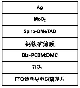
[0027] An n-type doped electron transport layer and TiO 2 The preparation method of the perovskite cell of layer comprises the following steps:

[0028] (1) FTO transparent conductive glass substrate cleaning and TiO 2 Film preparation: The FTO transparent conductive glass substrate was ultrasonically cleaned three times with deionized water, acetone, and ethanol, and then dried at 100°C until the solvent and moisture were completely removed. The treated FTO transparent conductive glass substrate was treated with a UV lamp and ozone for 25 min, and then deposited the electron transport layer TiO on the treated FTO transparent conductive glass substrate. 2 , placed in a 100°C oven for later use;

[0029] (2) Bis-PCBM and DMC composite film preparation: Dissolve 5mg Bis-PCBM in 2mL chlorobenzene, stir for 4h to get Bis-PCBM solution, then dissolve the dopant DMC in ethanol to prepare a precursor solution with a concentration of 0.2mg / mL, the precursor solution is doped in the...

Embodiment 2

[0036] An n-type doped electron transport layer and TiO 2 The preparation method of the perovskite cell of layer comprises the following steps:

[0037] (1) FTO transparent conductive glass substrate cleaning and TiO 2 Film preparation: The FTO transparent conductive glass substrate was ultrasonically cleaned three times with deionized water, acetone, and ethanol, and then dried at 100°C until the solvent and moisture were completely removed. The treated FTO transparent conductive glass substrate was treated with a UV lamp and ozone for 25 min, and then deposited the electron transport layer TiO on the treated FTO transparent conductive glass substrate. 2 , placed in a 100°C oven for later use;

[0038] (2) Bis-PCBM and DMC composite film preparation: Dissolve 5mg Bis-PCBM in 2mL chlorobenzene, stir for 4h to get Bis-PCBM solution, then dissolve the dopant DMC in ethanol to prepare a precursor solution with a concentration of 0.2mg / mL, the precursor solution is doped in the...

Embodiment 3

[0045] An n-type doped electron transport layer and TiO 2 The preparation method of the perovskite cell of layer comprises the following steps:

[0046] (1) FTO transparent conductive glass substrate cleaning and TiO 2 Film preparation: The FTO transparent conductive glass substrate was ultrasonically cleaned three times with deionized water, acetone, and ethanol, and then dried at 100°C until the solvent and moisture were completely removed. The treated FTO transparent conductive glass substrate was treated with a UV lamp and ozone for 25 min, and then deposited the electron transport layer TiO on the treated FTO transparent conductive glass substrate. 2 , placed in a 100°C oven for later use;

[0047] (2) Bis-PCBM and DMC composite film preparation: Dissolve 5mg Bis-PCBM in 2mL chlorobenzene, stir for 4h to get Bis-PCBM solution, then dissolve the dopant DMC in ethanol to prepare a precursor solution with a concentration of 0.2mg / mL, the precursor solution is doped in the...


PUM

PropertyMeasurementUnit
thicknessaaaaaaaaaa
thicknessaaaaaaaaaa

Abstract

The invention provides a preparation method of a perovskite battery with an n-type doped electron transport layer and a TiO2 layer. The method comprises the following steps of: (1) FTO transparent conductive glass substrate cleaning and TiO2 thin film preparation: an upper TiO2 layer is deposited on a treated FTO transparent conductive glass substrate, and the FTO transparent conductive glass substrate with the deposited upper TiO2 layer is arranged in a drying oven for later use; (2) Bis-PCBM and DMC composite film preparation; (3) spin coating treatment on the FTO transparent conductive glass substrate with the deposited upper TiO2 layer; (4) perovskite film preparation; (5) Spiro-OMeTAD thin film preparation: a Spiro-OMeTAD solution is spin coated on the FTO transparent conductive glass substrate in step (4); and (6) MoO3 and Ag electrode preparation: an MoO3 electrode and Ag electrode are formed on a Spiro-OMeTAD thin film through evaporation. With the method of the invention adopted, the electron mobility and conductivity of a thin film can be improved; the photoelectric conversion efficiency of a device can be improved; the surface of the thin film is smoother, so that the thin film can be used as a good substrate for the deposition and growth of a perovskite layer in subsequent processes; and the degradation process of the perovskite layer can be slowed down, and the stability of the device can be improved.

Description

technical field [0001] The invention belongs to the field of photovoltaic devices, in particular to an n-type doped electron transport layer and TiO 2 Layer perovskite cell fabrication method. Background technique [0002] Organic-inorganic hybrid perovskite solar cells are considered to be a form of energy comparable to inorganic silicon solar cells due to their unique optical properties and simple fabrication process. After several years of development, although its photoelectric conversion efficiency has exceeded 22%, manufacturing high-efficiency and long-term stable perovskite solar cells is a necessary condition for its commercialization. Perovskite solar cells have two types of device structures: planar and porous. Planar perovskite cells have attracted widespread attention due to their simple preparation process and low-temperature thin-film processing technology. In the planar structure, besides the perovskite layer itself, the structure of adjacent interfacial la...

Claims


Application Information

Patent Timeline
Patent Type & Authority Applications(China)
IPC IPC(8): H01L51/48H01L51/46H01L51/42
CPCH10K71/12H10K85/30H10K30/30H10K2102/00Y02E10/549
Inventor 王照奎廖良生叶青青
Owner SUZHOU UNIV
Why Eureka
Try Eureka