SiC-based GaN_HEMT back technology based on graphical slide

A backside process and patterning technology, which is applied in the fields of electrical components, semiconductor/solid-state device manufacturing, circuits, etc., can solve the problems of removal of etching by-products that affect the etching rate, affect the performance of front-side devices, and reduce the yield rate, etc., to achieve It is beneficial to device performance and yield, improves thermal conductivity, and reduces etching time

Active Publication Date: 2018-06-05
CHENGDU HIWAFER SEMICON CO LTD
View PDF5 Cites 6 Cited by
  • Summary
  • Abstract
  • Description
  • Claims
  • Application Information

AI Technical Summary

Problems solved by technology

[0004] In the back hole etching process, because the Si-C bond energy in the SiC substrate is relatively large, the SiC material is very hard, and the heat generated by high-power and long-time plasma etching is huge, and the heat dissipation problem will seriously affect the etching rate. And the removal of etching by-products directly leads to a decrease in yield and even affects the performance of front-side devices

Method used


Image

  • SiC-based GaN_HEMT back technology based on graphical slide
  • SiC-based GaN_HEMT back technology based on graphical slide
  • SiC-based GaN_HEMT back technology based on graphical slide

Examples


Embodiment

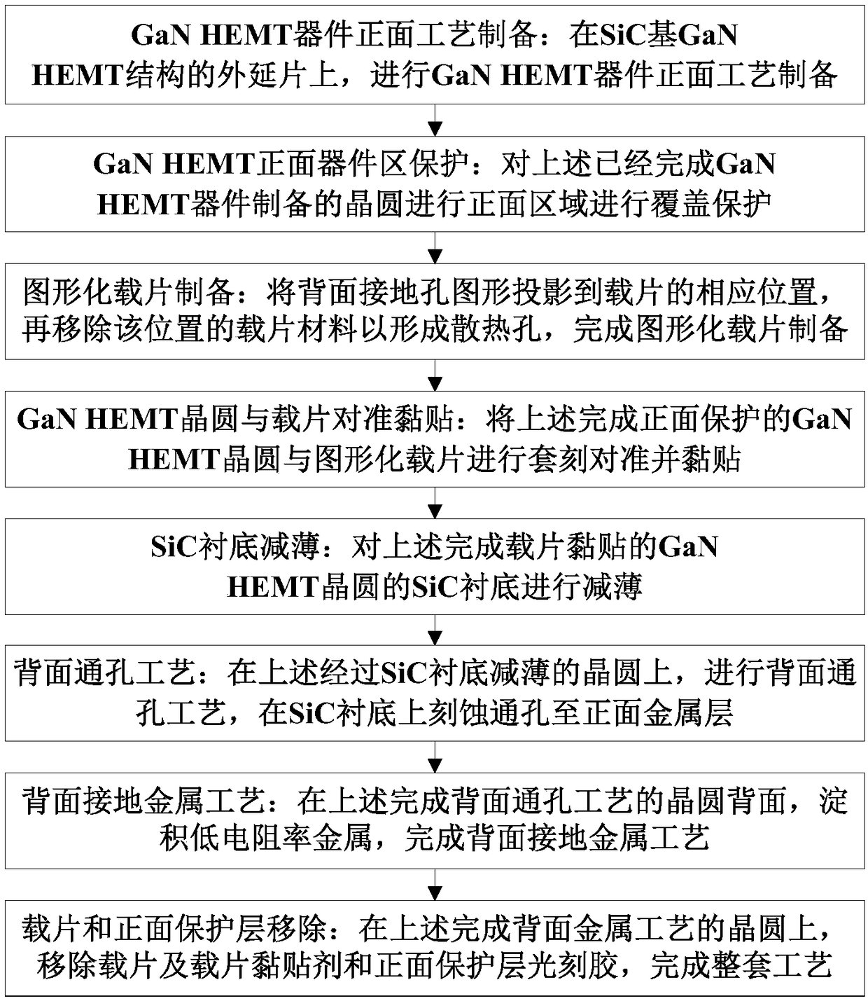
[0034] Such as Figure 1-9 As shown, an embodiment of a SiC-based GaN_HEMT backside process based on a patterned carrier of the present invention and a corresponding structural schematic diagram, the specific steps are as follows:

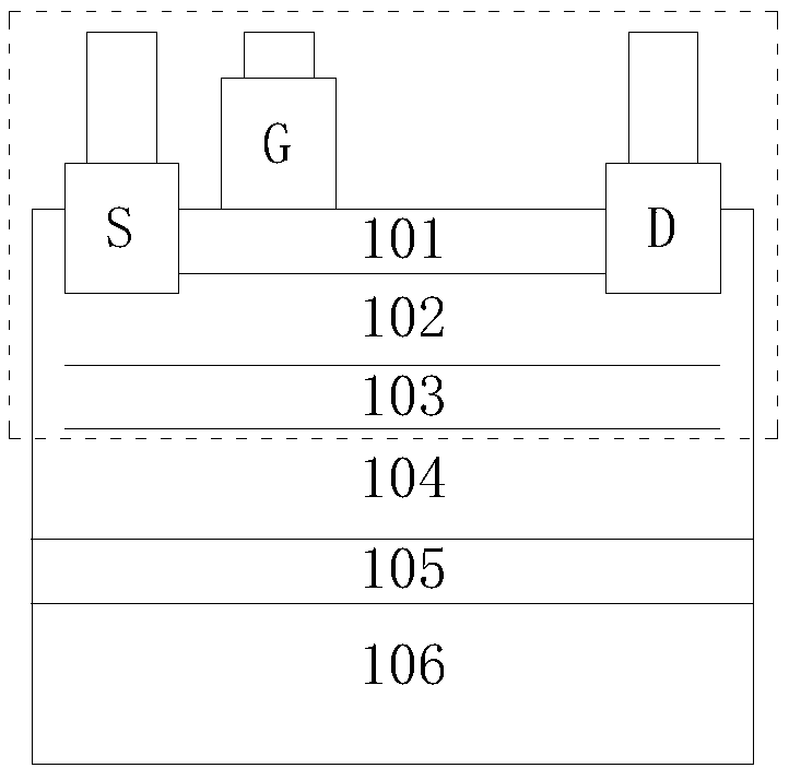
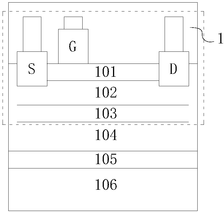
[0035] Step 1, front-side process preparation of GaN HEMT devices: On the epitaxial wafer of SiC-based GaN HEMT structure, the front-side process preparation of GaN HEMT devices is carried out.

[0036] On the epitaxial wafer of SiC-based GaN HEMT structure, the GaN HEMT device front-side process preparation is carried out. The preparation steps include but are not limited to, active area isolation, source and drain metal preparation, gate metal preparation, capacitor and inductor preparation, and electrode addition. Thick, metal interconnection and other related processes.

[0037] In one embodiment, on the epitaxial wafer of SiC-based GaN HEMT structure, device active region isolation is formed by fluorine ion implantation; Anneal in nitrogen a...


PUM


Abstract

The invention relates to a SiC-based GaN_HEMT back technology based on a graphical slide, and the technology comprises the following steps: carrying out the preparation of the front of a GaN HEMT device; protecting a front device region of the GaN HEMT device; preparing the graphical slide: projecting a background grounding hole pattern to be projected to a corresponding position of the slide, andremoving a slide material at the position so as to form a heat dissipation hole; carrying out the alignment and pasting of the GaN HEMT device and the graphical slide; thinning a SiC substrate; performing the back perforation process; performing the back grounding metal process; and removing the slide and the front protection layer. According to the invention, the slide material in a to-be-etchedSiC back hole region is removed or thinned on the slide at first, thereby forming the slide with the back hole pattern. Afterwards, the slide is enabled to be aligned with a GaN HEMT technology wafer, thereby effectively improving the thermal conduction capability of the whole wafer during the etching of SiC.

Description

technical field [0001] The invention relates to the technical field of compound semiconductor manufacturing, in particular to a SiC-based GaN_HEMT backside process based on a patterned carrier. Background technique [0002] As a representative device of the third-generation compound semiconductor, GaN HEMT devices are widely used in the field of microwave power amplification due to their high electron mobility, high breakdown voltage, high current density, and high reliability. The lattice constant of SiC material is close to that of GaN material, so high-quality GaN HEMT heterojunction structure is generally epitaxially grown on SiC substrate, which has a large current density, and the thermal conductivity of SiC material is high. , can guarantee the requirement of high power heat dissipation. [0003] In the device manufacturing process, after the front process is completed, the SiC substrate with a thickness of 500um must be thinned and back-holed. The SiC substrate with...

Claims


Application Information

Patent Timeline
Patent Type & Authority Applications(China)
IPC IPC(8): H01L21/3065H01L21/67H01L21/683H01L21/335
CPCH01L21/3065H01L21/67109H01L21/6835H01L29/66068
Inventor 林书勋
Owner CHENGDU HIWAFER SEMICON CO LTD
Why Eureka
Try Eureka