GaN power diode device with vertical structure and manufacturing method thereof

A technology of power diodes and manufacturing methods, which is applied in the direction of diodes, semiconductor/solid-state device manufacturing, semiconductor devices, etc., can solve problems such as difficult output current, complex flip-chip welding technology, and current congestion, so as to improve forward output current and Reverse blocking voltage, avoiding semiconductor material damage, and improving the effect of output current

Active Publication Date: 2020-11-20
INST OF MICROELECTRONICS CHINESE ACAD OF SCI
View PDF7 Cites 0 Cited by
  • Summary
  • Abstract
  • Description
  • Claims
  • Application Information

AI Technical Summary

Problems solved by technology

High-power gallium nitride-based diodes with a lateral structure using sapphire as the growth substrate have the advantages of large size, low cost, and good CMOS process compatibility, but it is difficult to obtain high output current, low heat dissipation efficiency, and current congestion. Low current density, high production cost, and inevitably suffer from problems such as high voltage current collapse caused by surface states
[0004] In the prior art, in order to solve the heat dissipation problem of high-power gallium nitride-based semiconductor diodes with a lateral structure, flip-chip welding technology has been proposed, but the flip-chip welding technology has complicated processes and high production costs
In addition, the substrate cost of GaN-based diodes with traditional vertical structures is extremely high, and the requirements for substrate lift-off technology are extremely high, which is not easy to realize

Method used


Image

  • GaN power diode device with vertical structure and manufacturing method thereof
  • GaN power diode device with vertical structure and manufacturing method thereof
  • GaN power diode device with vertical structure and manufacturing method thereof

Examples


Embodiment Construction

[0028] In order to make the purpose, technical solutions and advantages of the embodiments of the present invention clearer, the technical solutions in the embodiments of the present invention will be clearly and completely described below in conjunction with the drawings in the embodiments of the present invention. Obviously, the described embodiments It is only some embodiments of the present invention, but not all embodiments. Based on the embodiments of the present invention, all other embodiments obtained by persons of ordinary skill in the art without making creative efforts belong to the protection scope of the present invention.

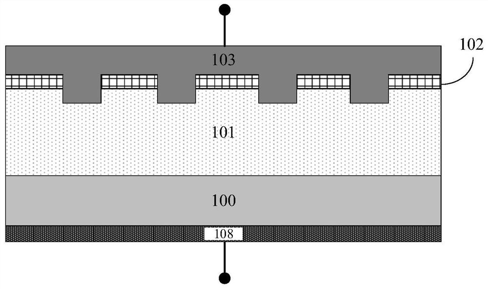
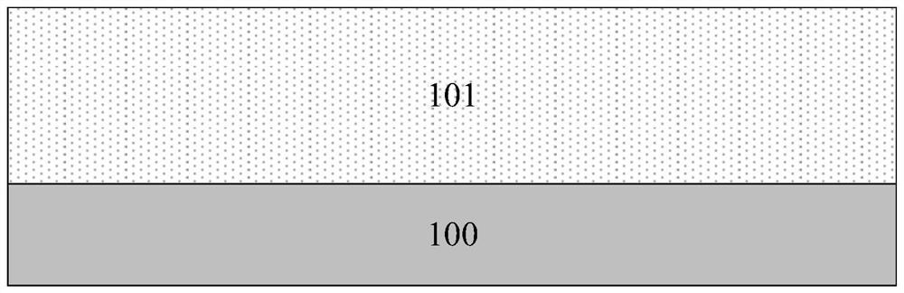
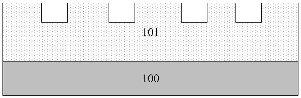
[0029] In a first aspect, the present invention provides a vertical gallium nitride (GaN) power diode device structure. figure 1 A schematic diagram showing the overall structure of a vertical GaN power diode device according to an embodiment of the present invention. As shown in the figure, 100 is heavily doped N + -GaN substrate, specific...


PUM


Abstract

The invention provides a fabrication method of a perpendicular-structure GaN power diode device. The fabrication method comprises the steps of 1, providing a substrate and an epitaxial layer on the substrate; 2, patterning a surface of the epitaxial layer, and etching grooves; 3, depositing first positive electrode metal on the surface of the epitaxial layer between the grooves; 4, covering the grooves and a surface of the first positive electrode metal with second positive electrode metal; and 5, fabricating a negative electrode on a back surface of the device. By the fabrication method, a forward output current and a reverse blocking voltage of the device can be increased, and the device performance of the GaN power diode is improved.

Description

technical field [0001] The invention relates to the technical field of semiconductors, in particular to a gallium nitride power diode device with a vertical structure and a manufacturing method thereof. Background technique [0002] Modern technology has continuously put forward higher requirements for the volume, reliability, withstand voltage and power consumption of semiconductor power devices. With the shrinking of the transistor feature size, due to the short channel effect and other physical laws and the limitation of production cost, the mainstream silicon-based materials and CMOS technology are developing to the 10nm process node and it is difficult to continue to improve. Gallium nitride has a wide band gap, high thermal conductivity, strong atomic bonds, good chemical stability, high operating temperature, high breakdown voltage, and strong radiation resistance. It is suitable for optoelectronics, high-temperature and high-power devices and Applications such as hi...

Claims


Application Information

Patent Timeline
Patent Type & Authority Patents(China)
IPC IPC(8): H01L21/329H01L29/861
CPCH01L29/66204H01L29/861
Inventor 康玄武刘新宇郑英奎黄森王鑫华魏珂
Owner INST OF MICROELECTRONICS CHINESE ACAD OF SCI
Why Eureka
Try Eureka