
Vacuum bonding method for full-color silicon-based oled microdisplay devices

A micro-display device, silicon-based technology, applied in semiconductor devices, electric solid-state devices, semiconductor/solid-state device manufacturing, etc., can solve the problems of high color filter material requirements, OLED material damage, etc. Good water and oxygen barrier performance, avoid the effect of color mixing

Active Publication Date: 2020-01-31
ANHUI SEMICON INTEGRATED DISPLAY TECH CO LTD
View PDF7 Cites 0 Cited by
  • Summary
  • Abstract
  • Description
  • Claims
  • Application Information

AI Technical Summary

Problems solved by technology

In comparison, the first production method is relatively simple in production process, and the precision is relatively easy to control, but it has higher requirements on the color filter material and requires it to be cured at a lower temperature. Generally, the curing temperature is required to be less than 120°, because Too high curing temperature will cause fatal damage to the OLED material; the second method of bonding can use the existing relatively mature color filter process to make a color filter film on glass and use a curing temperature of 230°C. temperature, but this solution has higher requirements on the accuracy of the bonding equipment and the bonding process

Method used


Image

  • Vacuum bonding method for full-color silicon-based oled microdisplay devices
  • Vacuum bonding method for full-color silicon-based oled microdisplay devices
  • Vacuum bonding method for full-color silicon-based oled microdisplay devices

Examples


Embodiment 1

[0050] This embodiment discloses a vacuum bonding method for a full-color silicon-based OLED microdisplay device, which includes the following steps:

[0051] Step 1, after cleaning the silicon substrate containing OLED and CMOS circuits and the color filter that have been encapsulated by thin film, drying;

[0052] Step 2, coating the frame sealant on the color filter, and coating the filling material on the silicon substrate containing OLED and CMOS circuits;

[0053] Step 3. Transfer the coated color filter and the silicon substrate to the vacuum chamber until the vacuum degree drops below 50Pa to carry out alignment bonding, and select several points on the bonded sample, and place the Spot UV pre-curing, UV illumination is 600mW / cm 2 above;

[0054] Step 4. Transfer the pre-cured sample to the UV irradiation device for UV curing, and set the UV illumination to 600mW / cm 2 ;

[0055] Step 5, cutting the cured sample into lobes to obtain the product.

[0056] Preferably...

Embodiment 2

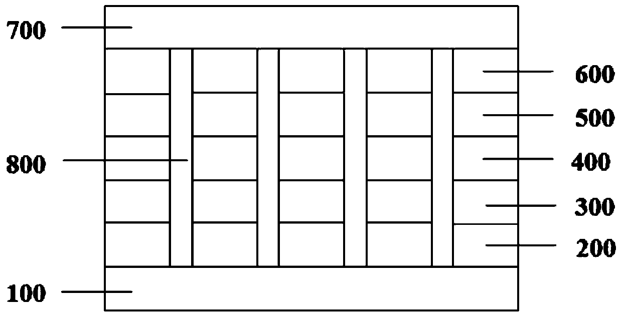
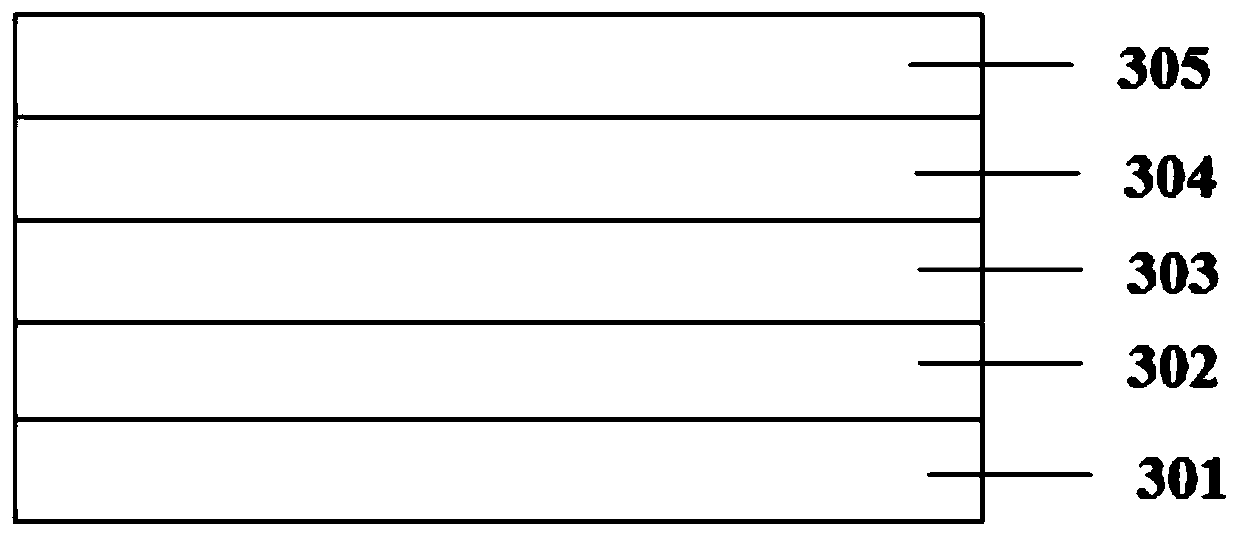
[0058] Such as Figure 1-3 As shown, the preparation method of the thin-film encapsulated silicon substrate containing OLED and CMOS circuits in Example 1 disclosed in this embodiment includes the following steps:

[0059] S1. Fabricate the pixel anode 200 on the CMOS circuit silicon substrate 100;

[0060] S2. Fabricate a reflective barrier layer 800 at the interval between adjacent pixel anodes 200;

[0061] S3. Using an organic layer mask, sequentially vapor-deposit a hole injection layer HIL301, a hole transport layer HTL302, a light emitting layer EML303, an electron transport layer ETL304, an electron injection layer EIL305, and a transparent cathode 400 on the pixel anode 200;

[0062] S4, encapsulating the film layer 500 on the transparent cathode 400;

[0063] S5, making a color photoresist layer 600 on the packaging film layer 500;

[0064] S6. Paste the cover glass 700 on the color photoresist layer 600;

[0065] S7. After cutting, a product is obtained.

[006...

Embodiment 3

[0073] Such as Figure 4-5 As shown, the preparation method of the thin-film encapsulated silicon substrate containing OLED and CMOS circuits in Example 1 disclosed in this embodiment includes the following steps:

[0074] S1. Fabricate the pixel anode on the silicon substrate of the CMOS circuit by magnetron sputtering.

[0075] S2. Place the donor element of the red OLED thermal transfer layer on the anode of the pixel, and use the laser beam to pass through the mask plate and the objective lens to form a square beam, and the laser beam will prepare the red OLED thermal transfer layer on the donor element Correspondingly transferred to the anode of the pixel to form a red OLED heat transfer layer 201 .

[0076] S4. Place the donor element of the green OLED thermal transfer layer on the anode of the pixel, use the laser beam to pass through the mask plate and the objective lens to form a square beam, and the laser beam will prepare the green OLED thermal transfer layer on th...


PUM

PropertyMeasurementUnit
thicknessaaaaaaaaaa
thicknessaaaaaaaaaa
thicknessaaaaaaaaaa

Abstract

The invention discloses a vacuum lamination method for a full-color silicon-based OLED microdisplay device, which comprises the following steps: step 1, after cleaning the silicon substrate containing OLED and CMOS circuits and the color filter that have been packaged in a thin film, drying Dry; Step 2, coating the frame sealant on the color filter, and coating the filling material on the silicon substrate containing OLED and CMOS; Step 3, transferring the coated color filter and the silicon substrate to In the vacuum chamber, wait for the vacuum degree to drop below 50Pa for alignment bonding, and select several points on the bonded samples, and perform UV pre-curing on the points, and the UV illumination is 600mW / cm 2 Above; step 4, transfer the pre-cured sample to the UV irradiation device for UV curing, and set the UV illumination to 600mW / cm 2 ; Step five, cutting the solidified sample into lobes to obtain the product.

Description

technical field [0001] The invention relates to the technical field of OLED microdisplay devices, in particular to a vacuum bonding method for full-color silicon-based OLED microdisplay devices. Background technique [0002] Silicon-based OLED (Organic Light Emitting Display) is known as the dark horse of next-generation display technology. It is different from conventional AMOLED devices that use amorphous silicon, microcrystalline silicon or low-temperature polycrystalline silicon thin-film transistors as backplanes. It is based on single-crystal silicon As an active organic light-emitting diode display device made of an active driving backplane, the pixel size is 1 / 10 of the traditional display device, and the fineness is much higher than that of the traditional device. It has high resolution, high integration, low power consumption, and small size. Small, light weight and many other advantages. Silicon-based OLED microdisplays have been widely used in military markets s...

Claims


Application Information

Patent Timeline
Patent Type & Authority Patents(China)
IPC IPC(8): H01L51/56H01L51/00H01L51/52H01L27/32H10K99/00
CPCH10K59/50H10K71/18H10K50/856H10K59/1201H10K71/00
Inventor 任清江李文连晋芳铭王仕伟赵铮涛
Owner ANHUI SEMICON INTEGRATED DISPLAY TECH CO LTD
Learn More