

Copper-selenium-based nano-composite thermoelectric material and preparation method thereof
A nano-composite, thermoelectric material technology, applied in thermoelectric device junction lead-out materials, thermoelectric device manufacturing/processing, nanotechnology, etc. Advanced problems, to achieve the effect of low cost, uniform distribution and good thermoelectric performance
- Summary
- Abstract
- Description
- Claims
- Application Information
AI Technical Summary
Problems solved by technology
Method used
Image

Examples
preparation example Construction
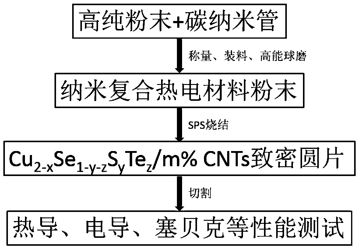
[0029] The preparation process of the present invention is realized through the processes of batching, ball milling (high energy ball milling) and discharge plasma sintering, figure 1 The process flow diagram for the preparation of this material is shown, specifically including: with the general formula Cu 2-x Se 1-y-z S y Te zThe stoichiometric ratio of / m%CNTs Weigh the high-purity powder of each element element and the carbon nanotubes with a mass percentage of m% as the initial raw materials. After weighing and charging, high-energy ball milling is performed to obtain nanocomposite thermoelectric material powder. The obtained nanocomposite thermoelectric material powder is then sintered by SPS to obtain a dense disc, and finally thermal conductivity, electrical conductivity, Seebeck and other performance tests are performed. The preparation method of the novel p-type nanocomposite thermoelectric material provided by the present invention is exemplarily described below....
Embodiment 1
[0037] Example 1: Cu 2 Se / 0.25%CNTs (x=0, y=0, z=0, m=0.25)
[0038] The high-purity powder raw materials Cu powder and Se powder were weighed at a molar ratio of 2:1, and then carbon nanotubes with a mass fraction of 0.25% were added. Then the powder raw material, carbon nanotubes and tungsten carbide balls were put into a ball mill jar made of tungsten carbide in an argon atmosphere glove box. The ball-to-material ratio is 10:1. Carry out high-energy ball milling again with the rotating speed of 500 revs per minute, and the ball milling time is 48 hours;
[0039] The nanocomposite material obtained by ball milling was subjected to spark plasma sintering (SPS sintering) at a sintering temperature of 480° C., a pressure of 65 MPa, and a sintering time of 5 minutes to obtain a dense bulk material.
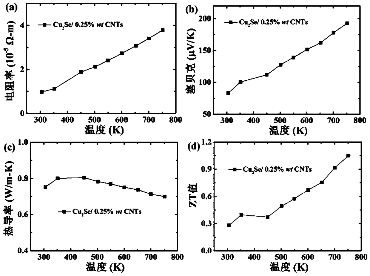
[0040] like figure 2 As shown, the resulting Cu 2 The measurement of thermoelectric properties of Se / 0.25%CNTs bulk material shows that the material has high Seebeck coefficie...
Embodiment 2
[0041] Example 2: Cu 2 Se / 0.5%CNTs (x=0, y=0, z=0, m=0.5)
[0042] The high-purity powder raw materials Cu powder and Se powder were weighed at a molar ratio of 2:1, and then carbon nanotubes with a mass fraction of 0.5% were added. Then the powder raw material, carbon nanotubes and tungsten carbide balls were put into a ball mill jar made of tungsten carbide in an argon atmosphere glove box. The ball-to-material ratio is 10:1. Carry out high-energy ball milling again with the rotating speed of 500 revs per minute, and the ball milling time is 48 hours;
[0043] The nanocomposite material obtained by ball milling was subjected to spark plasma sintering (SPS sintering) at a sintering temperature of 480° C., a pressure of 65 MPa, and a sintering time of 5 minutes to obtain a dense bulk material.
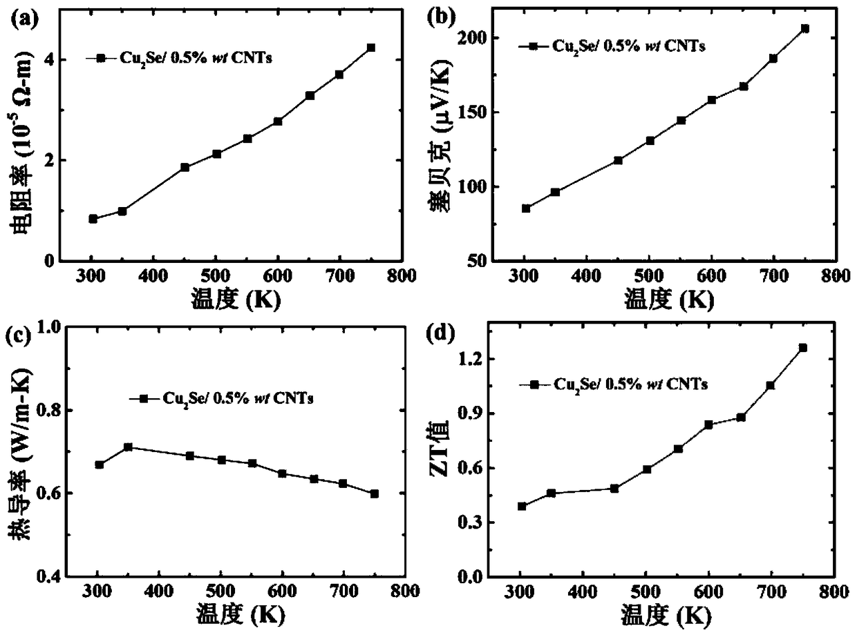
[0044] like image 3 As shown, the resulting Cu 2 The measurement of thermoelectric properties of Se / 0.5%CNTs bulk material shows that in the measured temperature range (300-750K)...
PUM
| Property | Measurement | Unit |
|---|---|---|
| Diameter | aaaaa | aaaaa |
| Length | aaaaa | aaaaa |
| Conductivity | aaaaa | aaaaa |
Abstract
Description
Claims
Application Information