Double-light beam micro/nano optical manufacturing method

An optical manufacturing and double-beam technology, which is applied in the fields of optics, nanotechnology, and optomechanical equipment, can solve the problems of small center distance, low pattern and structure feature density, and ultraviolet light energy loss, etc., to achieve strong mechanical strength, The effect of high feature sizes

Active Publication Date: 2018-07-13
HUAZHONG UNIV OF SCI & TECH
View PDF7 Cites 9 Cited by
  • Summary
  • Abstract
  • Description
  • Claims
  • Application Information

AI Technical Summary

Problems solved by technology

[0007] The existence of the diffraction limit restricts the fineness of micro-nano pattern and structure fabrication by light, which is mainly reflected in two aspects: first, it is difficult to make the feature size of the pattern and structure smaller, such as using visible light to fabricate patterns and structures, The diameter of the wire is difficult to be below 100 nanometers
The second is that the feature density of the manufactured pattern and structure is difficult to be small, that is, the distance between the centers of two physically separated straight lines in the manufactured pattern and structure is difficult to be small
However, these commonly used methods for manipulating visible light cause severe loss of UV energy due to the significant absorption of UV light by common materials.

Method used


Image

  • Double-light beam micro/nano optical manufacturing method
  • Double-light beam micro/nano optical manufacturing method
  • Double-light beam micro/nano optical manufacturing method

Examples


Embodiment 1

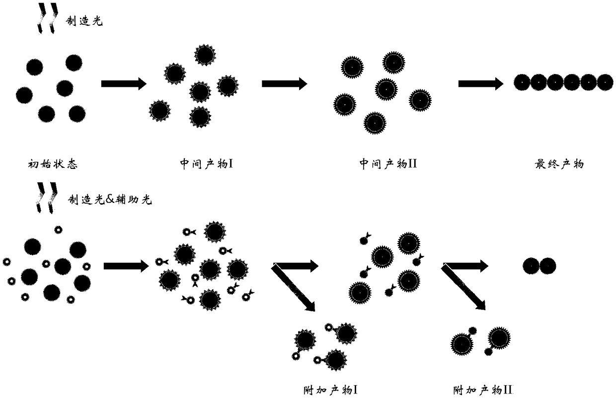
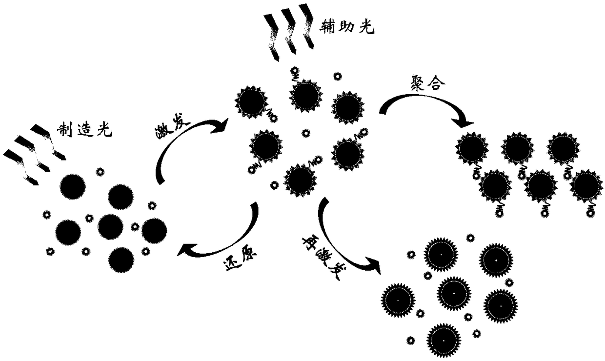
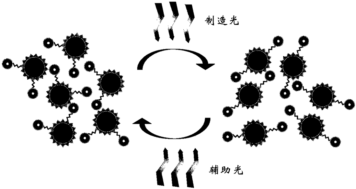
[0056] The present invention can be applicable to single-focus laser direct writing, such as Figure 4 As shown, the manufacturing light forms the optical path of the manufacturing light, and the auxiliary light forms the optical path of the auxiliary light. A beam expander E1 and a beam expander E2 are respectively placed in front of the manufacturing light and the auxiliary light, and the spatial phase modulators P1 and P2 are respectively placed after the beam expander. E1 and P1 are coaxially placed, and E2 and P2 are coaxially placed. The beam expansion and phase modulation of the manufacturing light and auxiliary light are combined by the dichroic mirror D. After the beam is combined, they are focused on the processing material to be irradiated through the objective lens at the same time. .

[0057] Single-focal feature size reduction can be achieved through the combined action of fabrication light and auxiliary light. Such as Figure 5 As shown in , the manufacturing...

Embodiment 2

[0061] The commonly used single-focus laser direct writing technology focuses a beam of light into the direct writing material and generally forms only a single focused spot. According to the method of the present invention applied to the multi-focus laser direct writing technology, by adjusting the light intensity, phase and polarization of the manufacturing light, a beam of light can be focused into the direct writing material to form multiple focused light spots. Generally, it can be realized by using a spatial light modulator to adjust the phase of light.

[0062] Multi-focus laser direct writing with Figure 4 The shown single-focus laser direct writing devices are the same, and it should be pointed out that the single-focus laser direct writing and multi-focus laser direct writing use different spatial phase modulators. Such as Figure 11 As shown, the manufactured light can also form multi-focus spots with Gaussian distribution after beam expansion and spatial phase m...

Embodiment 3

[0067] The invention can be applied to holographic grating manufacture. The holographic grating uses the principle of coherent superposition of light to image the interference fringes on the photosensitive material, and then dissolves the photosensitive (or non-photosensitive) part by developing technology to obtain a holographic grating. Such as Figure 16 As shown, in the manufacture of holographic gratings, two beams of light are formed by the manufacturing light and the auxiliary light respectively, and interference fringes are formed at the same position. The manufacturing light is divided into two beams with the same power by the beam splitter B1, and then passed by the beam expander E1 1 and E1 2 After the beam expands, they reach the mirror M1 respectively 1 and M1 2 , via M1 1 and M1 2 After reflection, it is focused on the photosensitive screen to form interference fringes; similarly, the auxiliary light is divided into two beams of equal power by the beam spli...


PUM


Abstract

The invention relates to a double-light beam micro/nano optical manufacturing method which comprises the following steps: S1, providing manufacturing light according to the material properties of a to-be-irradiated processing material, so that the material properties of the to-be-irradiated processing material is changed under the irradiation of the manufacturing light; S2, providing auxiliary light according to the material properties of the to-be-irradiated processing material, wherein the auxiliary light can hinder the change in the material properties of the to-be-irradiated material underthe irradiation of the manufactured light; S3, regulating and controlling the manufacturing light and the auxiliary light, so that focal points distributed on a first local light field and a second local light field and formed by the manufacturing light and the auxiliary light on the to-be-irradiated material overlap in space, and a processing light field which is not superimposed by the second local light field and acts on the to-be-irradiated processing material is formed in the range of the first local light field. The manufacturing method provided by the invention can realize smaller feature size and higher resolution ratio, and a pattern and a structure manufactured have better mechanical property.

Description

technical field [0001] The invention relates to the technical field of micro-nano optics manufacturing, in particular to a double-beam micro-nano optics manufacturing method. Background technique [0002] It is an ancient skill to use photosensitive materials to transfer designed graphics to corresponding substrates. Optical manufacturing originated from film photography technology 150 years ago, which was later applied to offset printing and PCB circuit board manufacturing, and then went deep into the fine processing of integrated circuits on silicon crystal materials at nanoscale dimensions. In addition to being widely used in integrated circuit manufacturing and flat panel display manufacturing industries, optical manufacturing technology has gradually extended to related fields such as micro-nano manufacturing, pharmaceutical research and development, micro-electromechanical systems, and fluid manufacturing in recent years. [0003] The method of using light irradiation...

Claims


Application Information

Patent Timeline
Patent Type & Authority Applications(China)
IPC IPC(8): G03F7/00B82Y40/00
CPCG03F7/00B82Y40/00
Inventor 甘棕松
Owner HUAZHONG UNIV OF SCI & TECH
Why Eureka
Try Eureka