Trench gate charge storage type IGBT (Insulated Gate Bipolar Translator) and manufacturing method thereof

A charge storage and charge storage layer technology, applied in circuits, electrical components, semiconductor/solid-state device manufacturing, etc., can solve problems such as increasing charge/discharge time, increasing device saturation current density, and affecting device switching loss compromise characteristics.

Active Publication Date: 2018-07-24
UNIV OF ELECTRONIC SCI & TECH OF CHINA
View PDF3 Cites 18 Cited by
  • Summary
  • Abstract
  • Description
  • Claims
  • Application Information

AI Technical Summary

Problems solved by technology

[0006] The implementation of method (1) will increase the gate-emitter capacitance and gate-collector capacitance at the same time, and the switching process of the IGBT is essentially the process of charging/discharging the gate capacitance, so the increase in the gate capacitance will Makes the charging/discharging time longer, which in turn causes the switching speed to decrease
Therefore, the deep trench gate depth will reduce the switching speed of the device, increase the switching loss of the device, and affect the compromise characteristics of the device's conduction voltage drop and switching loss; and the implementation of method (2) will increase the device's switching loss The gate capacitance will reduce the switching speed of the device and increase the switching loss, which will affect the compromise be

Method used


Image

  • Trench gate charge storage type IGBT (Insulated Gate Bipolar Translator) and manufacturing method thereof
  • Trench gate charge storage type IGBT (Insulated Gate Bipolar Translator) and manufacturing method thereof
  • Trench gate charge storage type IGBT (Insulated Gate Bipolar Translator) and manufacturing method thereof

Examples


Example Embodiment

[0098] Example 1:

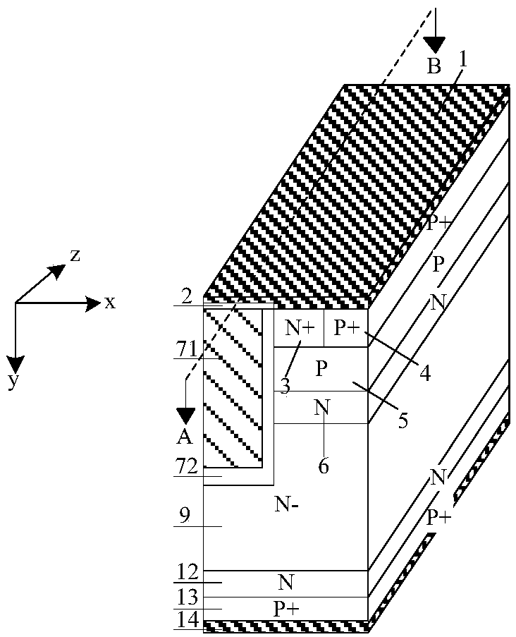
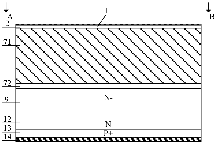
[0099] A trench gate charge storage type IGBT with one-half cell such as Figure 4 As shown, the section along the AB and CD lines is as Image 6 with Figure 7 As shown, a three-dimensional coordinate system is established with any inflection point of a half cell as the origin, and the two sides of the bottom surface of the quarter cell intersecting the inflection point are used as the x-axis and the z-axis respectively, passing the inflection point and The straight line perpendicular to the bottom surface is used as the y-axis, the direction of the x, y, and z-axis see Figure 4 ;

[0100] The one-half cell includes a collector metal 14, a P-type collector region 13, an N-type drift region 9 and an emitter metal 1 which are sequentially stacked from bottom to top; the top layer of the N-type drift region 9 has N-type charge storage layer 6, P-type base region 5, P+ body contact region 4, and N+ emitter region 3; said P-type base region 5 is located on the top ...

Example Embodiment

[0102] Example 2:

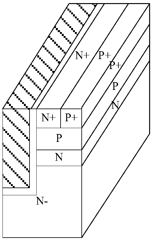
[0103] A trench gate charge storage type IGBT with one-half cell such as Figure 8 As shown, the cross-sections along the AB line, CD line, EF line and GH line are as follows Figure 10 to 13 As shown, the method of establishing the coordinate system is the same as that of Example 1, see Figure 8 ;

[0104] The difference between this embodiment and embodiment 1 is that the extension depth of the gate electrode 71 in the top layer of the N-type drift region 9 is equal to the extension depth of the split electrode 81, but the extension width of the gate electrode 71 at both ends of the top layer of the device is less than The extended width of the split electrode 81, while remaining part of the split electrode dielectric layer 82 and a part of the split electrode 81 structure on the top layer of the device; the thickness of the split electrode dielectric layer 82 is greater than the thickness of the gate dielectric layer 72.

[0105] In this embodiment, a portion ...

Example Embodiment

[0106] Example 3:

[0107] A trench gate charge storage type IGBT with one-half cell such as Figure 14 As shown, the cross-sections along the AB line, CD line, EF line and GH line are as follows Figure 16 to 19 As shown, the method of establishing the coordinate system is the same as that of Example 1, see Figure 14 ;

[0108] The difference between this embodiment and the second embodiment lies in that: this embodiment does not have a split electrode 81 and a split electrode dielectric layer 82 structure on the top layer of the device. The split electrode 81 and the split electrode dielectric layer 82 are located at the bottom of the gate electrode 71, and the N+ emitter region 3 The depth of the P+ body contact region 4 along the z-axis direction is equal and smaller than the depth of the P-type base region 5 along the z-axis direction. At the same time, the thickness of the gate electrode 71 connected to the N+ emitter region 3 through the gate dielectric layer 72 is greater t...


PUM

PropertyMeasurementUnit
Thicknessaaaaaaaaaa
Thicknessaaaaaaaaaa

Abstract

The invention relates to a trench gate charge storage type IGBT (Insulated Gate Bipolar Translator) and a manufacturing method thereof, and belongs to the technical field of power semiconductor devices. According to the invention, the extending depth of an emission region along the top layer of a base region in the traditional trench gate charge storage type IGBT structure is reduced, and a splittrench gate structure is introduced, wherein the split trench gate structure comprises a gate electrode, a gate dielectric layer at the periphery of the gate electrode, a split electrode which is located at the bottom of the gate electrode and connected through the gate dielectric layer and a split electrode dielectric layer located at the periphery of the split electrode, and the split electrodeis equipotential with emitter metal. The device structure provided by the invention improves a short-circuit safe working area and temperature characteristics of the device and the compromise betweenforward turn-on voltage drop Vceon and turn-off loss Eoff of the device while improving restrictions imposed on withstand voltage of the device by the doping concentration and thickness of the chargestorage layer, avoids current and voltage oscillation and EMI problems in the dynamic process of starting the device and improves the reliability of the device.

Description

technical field [0001] The invention belongs to the technical field of power semiconductor devices, in particular to a trench gate charge storage type insulated gate bipolar transistor (CSTBT). Background technique [0002] Insulated gate bipolar transistor (IGBT) is a new type of power electronic device developed based on the research of power MOSFET and power bipolar junction transistor (BJT), which is equivalent to a MOSFET driven by bipolar junction transistor (BJT). IGBT has the advantages of both power MOSFET structure and bipolar junction transistor (BJT) structure: it has the advantages of easy driving of power MOSFET, low input impedance and fast switching speed, and has the on-state current density of bipolar junction transistor (BJT) Large, low conduction voltage, low loss, and good stability. Based on these excellent device characteristics, IGBT has become a mainstream power device widely used in medium and high voltage fields in recent years, such as electric v...

Claims


Application Information

Patent Timeline
IPC IPC(8): H01L29/739H01L21/331H01L29/06H01L29/423
CPCH01L29/0603H01L29/0684H01L29/4236H01L29/66325H01L29/7393
Inventor 张金平赵倩赵阳刘竞秀李泽宏张波
Owner UNIV OF ELECTRONIC SCI & TECH OF CHINA
Why Eureka
Try Eureka