Method for preparing N-doped graphene through ion implantation

A technology of nitrogen-doped graphene and ion implantation, which is applied in semiconductor/solid-state device manufacturing, electrical components, circuits, etc. Poor electrical properties of doped graphene

Inactive Publication Date: 2018-08-03
PEKING UNIV
View PDF5 Cites 0 Cited by
  • Summary
  • Abstract
  • Description
  • Claims
  • Application Information

AI Technical Summary

Problems solved by technology

This method will be affected by factors such as gas flow velocity, growth temperature, growth time and catalytic substrate, and it is difficult to precisely control the form and amount of doping
[0005] 2. Irradiation or plasma treatment method: This method directly uses low-energy ions or plasma to bombard graphene, so as to achieve the purpose of replacement doping, but due to the low efficiency of N atom replacement doping, the bombardment will also lead to more Many point defects affect the electrical properties of graphene materials
The doping amount and controllability of this method are very poor, and it is difficult to prepare large-area graphene materials, which cannot meet the requirements of nanoelectronics
[0007] In summary, the methods for preparing nitrogen-doped graphene in the prior art all have the problem that the amount of nitrogen doping is uncontrollable, and the electrical properties of the prepared nitrogen-doped graphene are poor.

Method used


Image

  • Method for preparing N-doped graphene through ion implantation
  • Method for preparing N-doped graphene through ion implantation
  • Method for preparing N-doped graphene through ion implantation

Examples


Embodiment 1

[0061] Preparation of multilayer film samples:

[0062] SiO by magnetron sputtering 2 / Si substrate coated with 40nm a-SiC (amorphous silicon carbide) film (background vacuum 10 - 5 Pa, deposition rate 0.3As -1 );

[0063] Then, on the above-mentioned coated substrate, 100nm Cu and 250nmNi films were sequentially plated on the basis of the a-SiC film by using filtered cathodic vacuum arc deposition (FCVA) (background vacuum 10 -3 Pa, the deposition rate is 0.5As, respectively -1 , 0.2As -1 ).

[0064] Ion Implantation:

[0065] N ion implantation parameters:

[0066] Vacuum (1×10 -3 Pa), energy (40keV), dose 5×10 15 ions cm -2 .

[0067] Rapid annealing:

[0068] The heating rate was 90°C / s, the annealing temperature was 800°C, and the annealing time was 3min, and NG was prepared.

[0069] Test Results:

[0070] N doping amount 0.5at%, electron mobility 800cm 2 V -1 the s -1 .

Embodiment 2

[0072] Preparation of multilayer film samples:

[0073] SiO by magnetron sputtering 2 / Si substrate coated with 20nm a-SiC (amorphous silicon carbide) film (background vacuum 10 - 5 Pa, deposition rate 0.3As -1 );

[0074] Then, on the above-mentioned coated substrate, utilize filter cathodic vacuum arc coating technology (FCVA) to plate 50nm Cu and 200nmNi thin films successively on the basis of a-SiC film (background vacuum 10 -3 Pa, the deposition rate is 0.5As, respectively -1 , 0.2As -1 ).

[0075] Ion Implantation:

[0076] N ion implantation parameters:

[0077] Vacuum (8×10 -4 Pa), energy (40keV), dose 4×10 15 ions cm -2 .

[0078] Rapid annealing:

[0079] The heating rate was 50°C / s, the annealing temperature was 800°C, and the annealing time was 3min, and NG was prepared.

[0080] Test Results:

[0081] N doping amount 0.4at%, electron mobility 850cm 2 V -1 the s -1 .

Embodiment 3

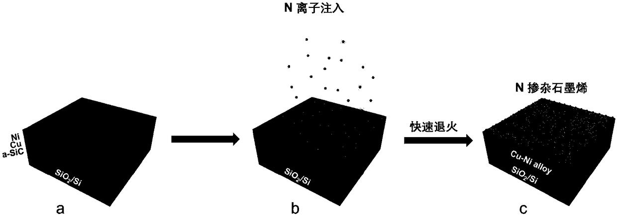
[0083] The preparation process of this embodiment is as follows image 3 As shown, there are three steps:

[0084] Preparation of multilayer film samples:

[0085] SiO by magnetron sputtering 2 / Si substrate coated with 30nm a-SiC (amorphous silicon carbide) film (background vacuum 10 - 5 Pa, deposition rate 0.3As -1 )

[0086] Then, on the above-mentioned coated substrate, utilize filter cathodic vacuum arc coating technology (FCVA) to sequentially plate 100nm Cu and 300nmNi thin films on the basis of a-SiC thin films (background vacuum 10 -3 Pa, the deposition rate is 0.5As, respectively -1 , 0.2As -1 ).

[0087] Ion Implantation:

[0088] N ion implantation parameters:

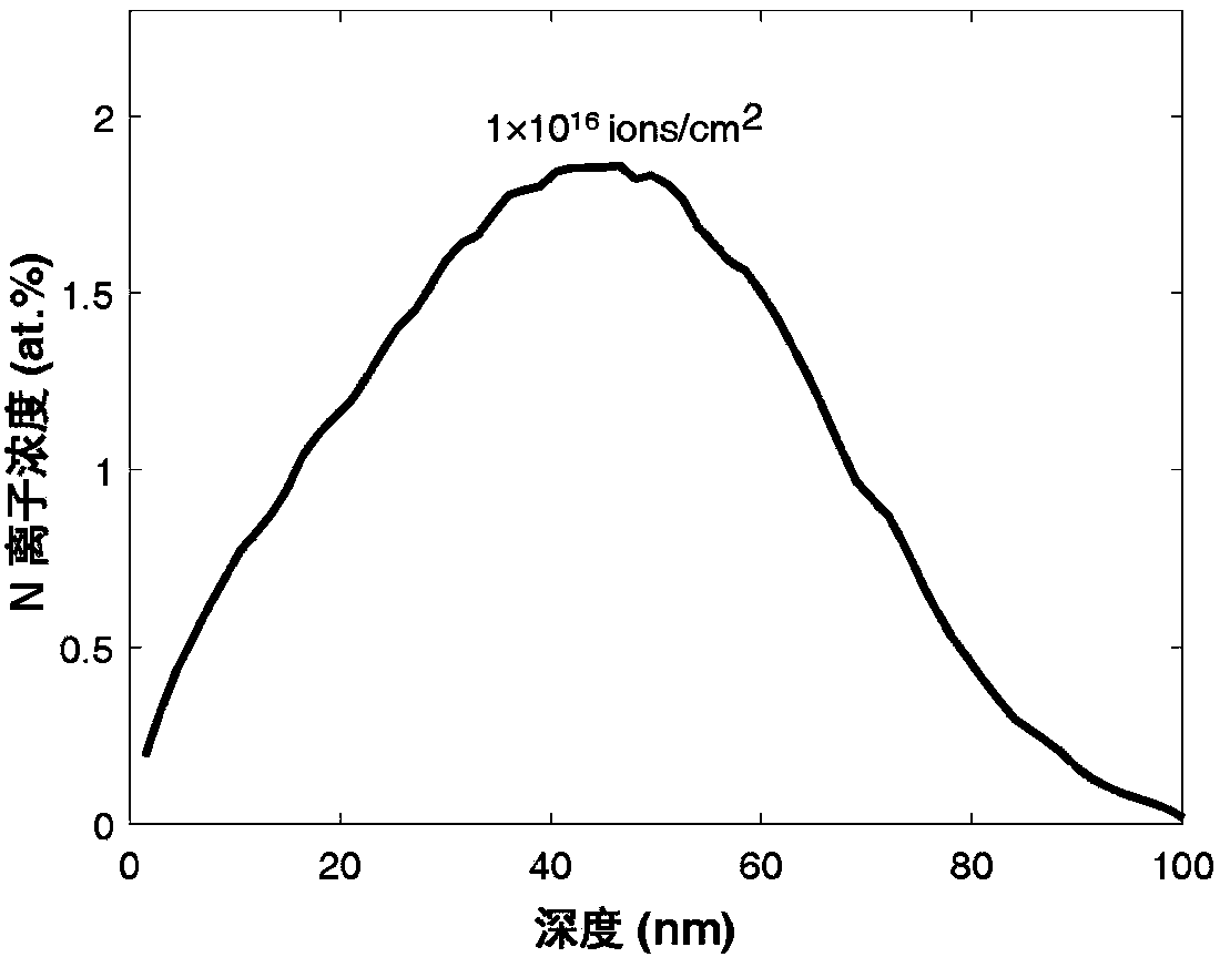
[0089] Vacuum (8×10 -4 Pa), energy (40keV), dose 1×10 16 ions cm -2 .

[0090] Rapid annealing:

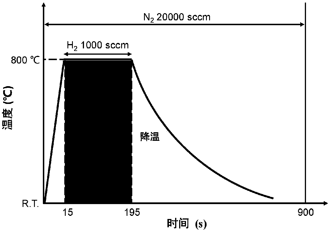
[0091] The annealing process curve is as figure 2 As shown, the heating rate is 70°C / s, the annealing temperature is 800°C, and the annealing time is 3min, and NG is prepared.

[0092] Test Re...


PUM

PropertyMeasurementUnit
Thicknessaaaaaaaaaa
Thicknessaaaaaaaaaa
Thicknessaaaaaaaaaa

Abstract

The invention provides a method for preparing N-doped graphene through ion implantation, and the method comprises the following steps: providing a multilayer film substrate which comprises a Si layer,a SiO2 layer, an amorphous SiC layer, a Cu layer and a Ni layer, wherein the Si layer, the SiO2 layer, the amorphous SiC layer, the Cu layer and the Ni layer are sequentially set, and the amorphous SiC layer can be replaced by a DLC film; carrying out the implantation of nitrogen ions on the surface of the Ni layer of the multilayer film substrate, and obtaining an N-doped substrate; carrying outthe annealing of the N-doped substrate, and obtaining N-doped graphene. According to the invention, the method combines the ion implantation technology and a solid state carbon source method, takes amorphous SiC or the DLC film as a carbon source, enables the nitrogen atoms and carbon atoms to be segregated through the ion implantation, and further achieves the preparation of the N-doped graphene. The method achieves the control of a doping quantity of nitrogen atoms through the control of the ion implantation parameter. An experiment result indicates that the method can achieve the precise control of the doping quantity of the nitrogen atoms, and the electronic mobility of the obtained N-doped graphene can reach 850cm<2>V<-1>s<-1>.

Description

technical field [0001] The invention relates to the technical field of graphene preparation, in particular to a method for preparing nitrogen-doped graphene by ion implantation. Background technique [0002] Graphene is a new type of two-dimensional material. Due to its excellent properties in mechanical, optical, electrical and chemical aspects, graphene materials have great application potential. However, the valence band and conduction band of intrinsic graphene are conically contacted in the center of the Brillouin zone. It is a semiconductor or semi-metal with zero band gap, which cannot be turned off, which limits its application in nanoelectronics. Therefore, it is of great significance to open the band gap of intrinsic graphene. Doping is the most common method to modulate the electrical properties of graphene, and the common doped heteroatoms are mainly N (nitrogen) and B (boron). [0003] At present, the research on nitrogen-doped graphene mainly includes the fol...

Claims


Application Information

Patent Timeline
IPC IPC(8): H01L21/02H01L21/265H01L21/324
CPCH01L21/02381H01L21/02488H01L21/02527H01L21/0257H01L21/02612H01L21/26506H01L21/324
Inventor 赵子强赵云彪付恩刚王绪韩冬
Owner PEKING UNIV
Why Eureka
Try Eureka