

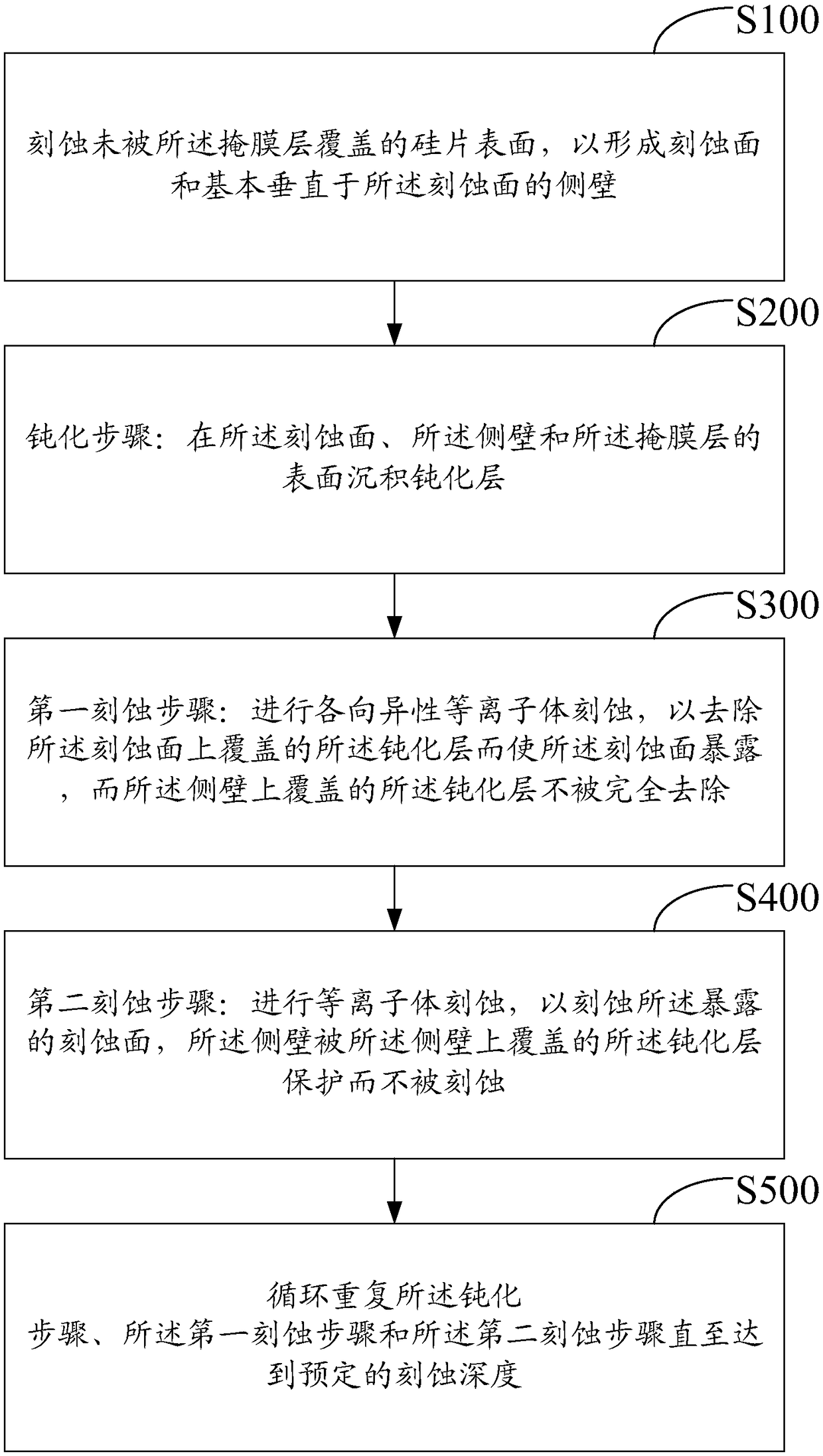
Deep Si etching method
A deep silicon etching and surface etching technology, applied in decorative arts, gaseous chemical plating, microstructure technology, etc., can solve the problems of reduced etching rate, sidewall damage, increased line width loss, etc.
- Summary
- Abstract
- Description
- Claims
- Application Information
AI Technical Summary
Problems solved by technology
Method used
Image

Examples
Embodiment 1
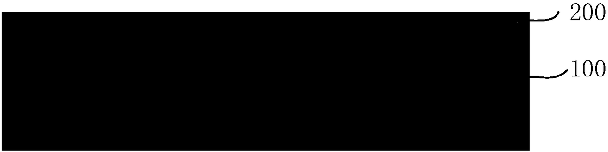
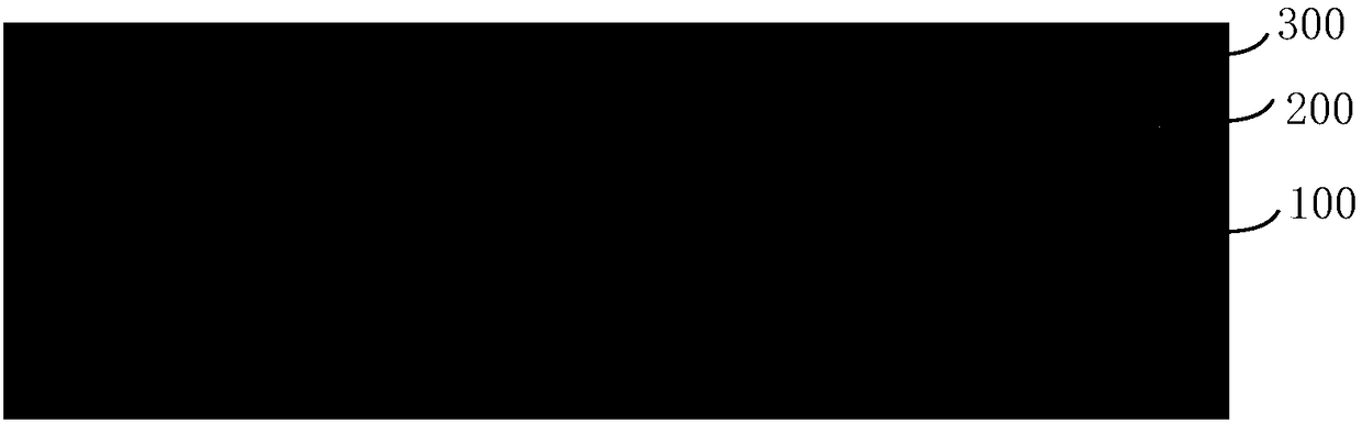
[0074] Embodiment 1 prepares the base material that covers patterned mask layer on the silicon wafer
[0075] Step 1: Prepare Silicon Wafer Material
[0076] The specifications of the prepared silicon wafer are N-type 100 crystal orientation, thickness 400um, resistivity 0.002-0.005Ω·m. And use a laser marking machine to mark and number the silicon wafers (the marking side is the back side, and the non-marking side is the front side) for subsequent data recording.
[0077] Step Two: Clean the Wafer
[0078] Silicon wafers are cleaned with standard RCA before use. Put the glass sheet in the mixed solution of sulfuric acid:hydrogen peroxide=4:1 and wash it for 5 minutes, and rinse it with deionized water for 5 times; Rinse with deionized water for 5 times; then wash in a mixed solution of hydrochloric acid: hydrogen peroxide: deionized water = 1:1:4 for 5 minutes, rinse with deionized water for 5 times; dry at 2000 rpm for 5 minutes.
[0079] Step 3: Preparation of SiO 2 ha...
Embodiment 2
[0085] Embodiment 2 deep silicon etching process
[0086] Using equipment SPTS LPX ICP-SR, using the process parameters shown in Table 1, the substrate provided in Example 1 was etched on silicon wafers.
[0087] Table 1 Parameter table of deep silicon etching process
[0088]
[0089] The deep silicon etching process was carried out 920 cycles in total, and the passivation time of the passivation step increased at a uniform speed with the increase of the number of cycles, and the rate of increase was 2.17×10 -4 s / period, increased from 2.2s to 2.4s; the etching time of the second etching step increases at a uniform speed as the number of cycles increases, and the rate of increase is 2.06×10 -3 s / period, increased from 0.8s to 2.7s; the electric plate plate power of the second etching step increases at a uniform speed with the increase of the number of cycles, and the increase rate is 1.09×10 -2 W / cycle, increased from 50W to 60W; the gas pressure of the second etching st...
PUM
| Property | Measurement | Unit |
|---|---|---|
| Thickness | aaaaa | aaaaa |
| Resistivity | aaaaa | aaaaa |
| Opening width | aaaaa | aaaaa |
Abstract
Description
Claims
Application Information