Perovskite/silicon heterojunction stacked solar cell structure and manufacturing method thereof
A stacked battery and silicon heterojunction technology, which is applied in circuits, photovoltaic power generation, electrical components, etc., can solve problems affecting the long-term stability of batteries, high cost, and difficulties in mass production of stacked batteries, and achieve high-efficiency metallization Solution, reduce battery production cost, improve the effect of battery stability
- Summary
- Abstract
- Description
- Claims
- Application Information
AI Technical Summary
Problems solved by technology
Method used
Image

Examples
specific Embodiment 1
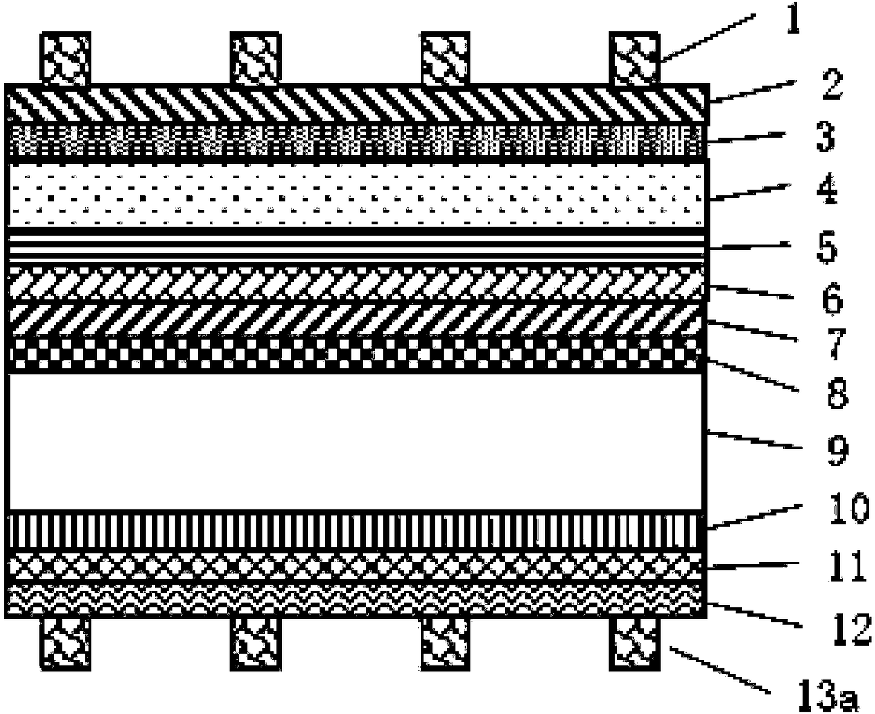
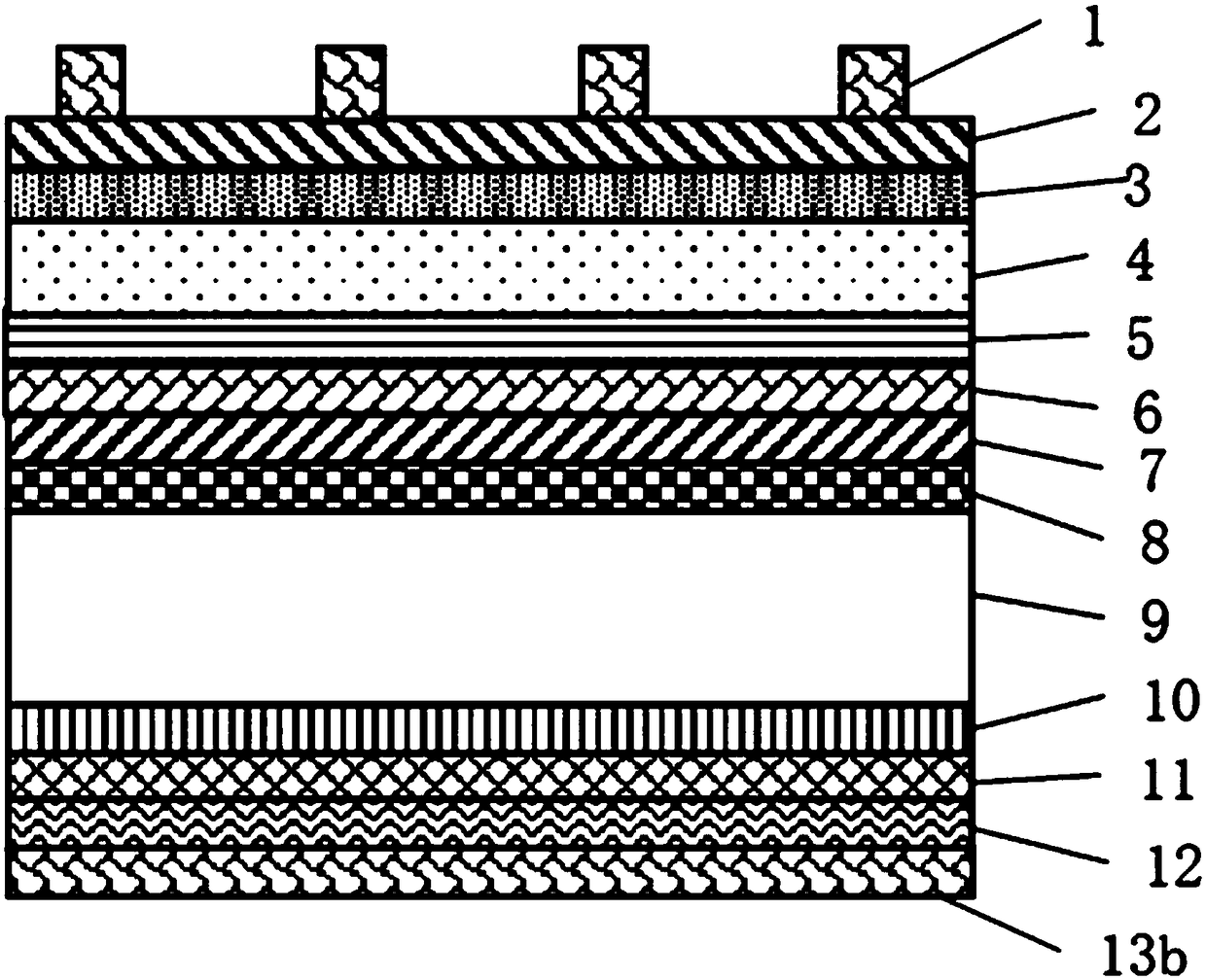
[0035] A method for manufacturing a perovskite / silicon heterojunction solar cell structure, comprising the following steps:
[0036] Step 1, making the single crystal silicon layer 9, etching the n-type polished single crystal silicon substrate with a thickness of 90-250 μm in a KOH solution to obtain a pyramid structure surface, the temperature of the solution is about 90°C, and cleaning the silicon wafer after the completion, Here, the thickness of the n-type polished single crystal silicon substrate is preferably 150 μm.
[0037] In step 2, the intrinsic amorphous silicon film 10 and the p-type or n-type amorphous silicon film 11 are sequentially deposited on the back of the single crystal silicon layer 9 by plasma enhanced chemical vapor deposition (PECVD). Wherein the thickness of the lower intrinsic amorphous silicon film 10 (a-Si:H(i)) is 3-10 nm, preferably 5 nm here; the p-type or n-type amorphous silicon film 11 is selected as the n-type amorphous silicon film, n-ty...
specific Embodiment 2
[0048] Step 1, making the single crystal silicon layer 9, etching the n-type polished single crystal silicon substrate with a thickness of 90-250 μm in a KOH solution to obtain a pyramid structure surface, the temperature of the solution is about 90°C, and cleaning the silicon wafer after the completion, Here, the thickness of the n-type polished single crystal silicon substrate is preferably 250 μm.
[0049] In step 2, the intrinsic amorphous silicon film 10 and the p-type or n-type amorphous silicon film 11 are sequentially deposited on the back of the single crystal silicon layer 9 by plasma enhanced chemical vapor deposition (PECVD). Wherein the thickness of the lower intrinsic amorphous silicon film 10 (a-Si:H(i)) is 3-10 nm, preferably 5 nm here; the p-type or n-type amorphous silicon film 11 is selected as the p-type amorphous silicon film, p-type amorphous silicon thin film (a-Si:H(p + )) has a thickness of 3 to 30 nm, preferably 20 nm.
[0050] Step 3: Deposit an in...
specific Embodiment 3
[0060] Step 1, making the single crystal silicon layer 9, etching the n-type polished single crystal silicon substrate with a thickness of 90-250 μm in a KOH solution to obtain a pyramid structure surface, the temperature of the solution is about 90°C, and cleaning the silicon wafer after the completion, Here, the thickness of the n-type polished single crystal silicon substrate is preferably 250 μm.
[0061] In step 2, the intrinsic amorphous silicon film 10 and the p-type or n-type amorphous silicon film 11 are sequentially deposited on the back of the single crystal silicon layer 9 by plasma enhanced chemical vapor deposition (PECVD). Wherein the thickness of the lower intrinsic amorphous silicon film 10 (a-Si:H(i)) is 3-10 nm, preferably 5 nm here; the p-type or n-type amorphous silicon film 11 is selected as the p-type amorphous silicon film, p-type amorphous silicon thin film (a-Si:H(p + )) has a thickness of 3 to 30 nm, preferably 20 nm.
[0062] Step 3: Deposit an in...
PUM
| Property | Measurement | Unit |
|---|---|---|
| Thickness | aaaaa | aaaaa |
| Thickness | aaaaa | aaaaa |
| Thickness | aaaaa | aaaaa |
Abstract
Description
Claims
Application Information