3D integrated circuit through silicon via fault detection system and detection method

An integrated circuit and fault detection technology, which is applied in the direction of electronic circuit testing, measuring electronics, measuring devices, etc., can solve the problems of low test accuracy, high-density TSV array testing difficulty, and occupying a large area, etc., to achieve a simple circuit structure Effect

Inactive Publication Date: 2018-12-14
XIAN UNIV OF TECH
View PDF5 Cites 3 Cited by
  • Summary
  • Abstract
  • Description
  • Claims
  • Application Information

AI Technical Summary

Problems solved by technology

For example, test the RC delay time of TSV or simulate the amplifier to detect TSV failure or compare the voltage on the TSV to be tested with the reference voltage to judge the failure, etc. These methods usually need to set the reference voltage, and can only distinguish between greater than or less than the threshold voltage. state, the test accuracy is very low
There are also literatures that propose an all-digital BIST structure based on a ring oscillator, a BIST test structure based on signal bounce, etc. These methods usually require the test circuit to be built in the chip under test and occupy a large area, while the area of ​​a high-density TSV array Very limited resources make it difficult to test large-scale, high-density TSV arrays

Method used


Image

  • 3D integrated circuit through silicon via fault detection system and detection method
  • 3D integrated circuit through silicon via fault detection system and detection method
  • 3D integrated circuit through silicon via fault detection system and detection method

Examples


Embodiment 1

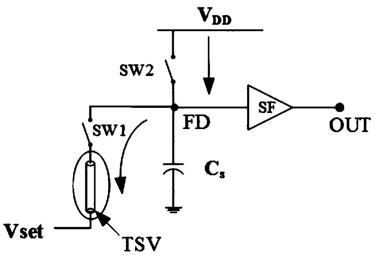
[0036] The invention provides a 3D integrated circuit through-silicon via fault detection system, such as figure 1 shown, the first switch SW1 and capacitor C S , the first switch SW1 connects the capacitor C S The upper plate FD, capacitance C S The upper plate FD of is connected with the second switch SW2 and the source follower SF, the capacitor C S The lower plate is grounded.

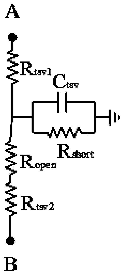
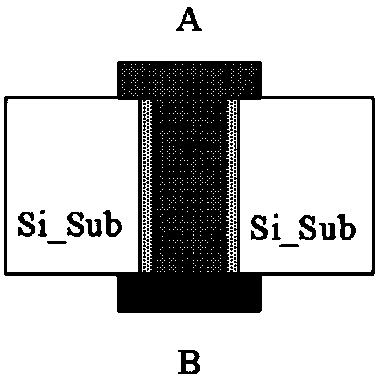
[0037] Such as figure 2 As shown, the TSV includes a metal conductive cylinder whose outer wall is coated with an insulating layer. The defect of TSV is caused by the instability that may exist in the process during processing. The normal TSV silicon chip is insulated from the substrate through the insulating layer of the side wall, and the A and B ends of the metal conductive cylinder have good conductivity and low resistance. If there is a breakdown or defect in the insulating layer of the TSV, the metal conductive cylinder of the TSV passes through the insulating layer. This defect is usu...

Embodiment 2

[0047] TSV fault response electric signal readout array implementation scheme, as follows:

[0048] The value of the capacitor Cs in the readout circuit has a great influence on the discharge time, and the larger the value of the capacitor Cs, the wider range of TSV resistance characteristics the readout circuit can distinguish. When the value of the capacitor Cs is large enough, the resistance characteristics of the TSV without failure can be evaluated; however, since the on-chip capacitor Cs occupies a large area, it is difficult to integrate a large capacitor in a limited area.

[0049] In order to solve the detection of multiple TSVs, reduce the large area occupied by the on-chip capacitor, integrate a large capacitor in a limited area, and share the capacitor Cs, such as Figure 4 As shown in , an example of a circuit is given; for a high-density TSV array (assuming there are i TSVs), one end of each TSV passes through its corresponding MOS switch (by Rst_n Control) conn...

Embodiment 3

[0051] Implementation scheme of readout electrical signal array device and TSV position matching

[0052] Due to the small scale and spacing of TSV, the electrical signal of the high-density TSV through-hole is read by the electrode lattice, specifically: the response electrical signal readout circuit array is designed using the same process as the TSV to be tested, and at the same time as the TSV is prepared, Complete readout array preparation. An electrode lattice is designed on the top layer of the readout circuit array, and the lattice adopts the same layout as the high-density TSV array. During the test, real-time online TSV fault test and diagnosis can be realized by using the existing alignment technology on the existing production line. The electrode plate applies an electrical signal to the TSV, and uses the TSV response electrical signal readout circuit based on charge charging and discharging to read the response signal from the lower electrode of the TSV, and ...


PUM


Abstract

The invention discloses a 3D integrated circuit through silicon via (TSV) fault detection system and a test and diagnosis method thereof, comprising a capacitor, an upper polar plate of the capacitoris connected with a first switch composed of multiple branch circuits in parallel, and the upper polar plate of the capacitor is also connected with a second switch and a source follower; and a lowerpolar plate of the capacitor is earthed. A voltage signal is applied by virtue of a TSV of the upper polar plate of the capacitor, the source follower reads the voltage signal, and whether the TSV isnormal or not is judged according to reduced amplitude of the voltage signal. The system and the method which are disclosed by the invention can analyze electrical properties of the TSV and realize test, location and grading on open circuit and short circuit defects of the TSV; circuit structure is simple, and a voltage reference and a test circuit do not need to be externally connected; and the system and the method which are disclosed by the invention adopt the same detection circuit, short circuit and open circuit fault detection on the TSV can be completed by setting a test mode, and especially online test and diagnosis on a high-density TSV array can be realized.

Description

technical field [0001] The invention belongs to the technical field of integrated circuit testing, and relates to a 3D integrated circuit through-silicon hole fault detection system and a detection method. Background technique [0002] Three-dimensional integration based on TSV is the key technology to realize high-performance integrated circuits in the future; TSV testing is the bottleneck point restricting the industrialization of three-dimensional integrated circuits. First, defects or blemishes may occur in the TSV manufacturing stage due to process or pollution, etc., resulting in different types and degrees of faults in the circuit. However, there are no practical testing methods and tools for online detection of faulty TSVs in the prior art. Second, with the improvement of the integration of three-dimensional integrated circuits, TSV technology will develop in the direction of miniaturization in terms of the number of stacked layers in the vertical direction, the thic...

Claims


Application Information

Patent Timeline
Patent Type & Authority Applications(China)
IPC IPC(8): G01R31/28G01R31/02
CPCG01R31/2851G01R31/50
Inventor 戴力余宁梅
Owner XIAN UNIV OF TECH
Why Eureka
Try Eureka