Shield gate power device

A technology of power devices and shielding grids, which is applied in the direction of semiconductor devices, electrical components, circuits, etc., can solve the problems of device cell density and current capacity limitations, achieve industrial production, improve cell density and current capacity, and achieve low conductivity. The effect of on-resistance

Inactive Publication Date: 2019-01-08
UNIV OF ELECTRONIC SCI & TECH OF CHINA
View PDF3 Cites 7 Cited by
  • Summary
  • Abstract
  • Description
  • Claims
  • Application Information

AI Technical Summary

Problems solved by technology

However, in order to improve the reliability of the lower oxide layer and reduce the output capacitance to ensure that it has a certain withstand voltage capability, the insulating dielectric layer around the lower polycrystalline "body field plate" is generally thicker, due to the high depth and width of etching and filling The speci

Method used


Image

  • Shield gate power device
  • Shield gate power device
  • Shield gate power device

Examples


Embodiment 1

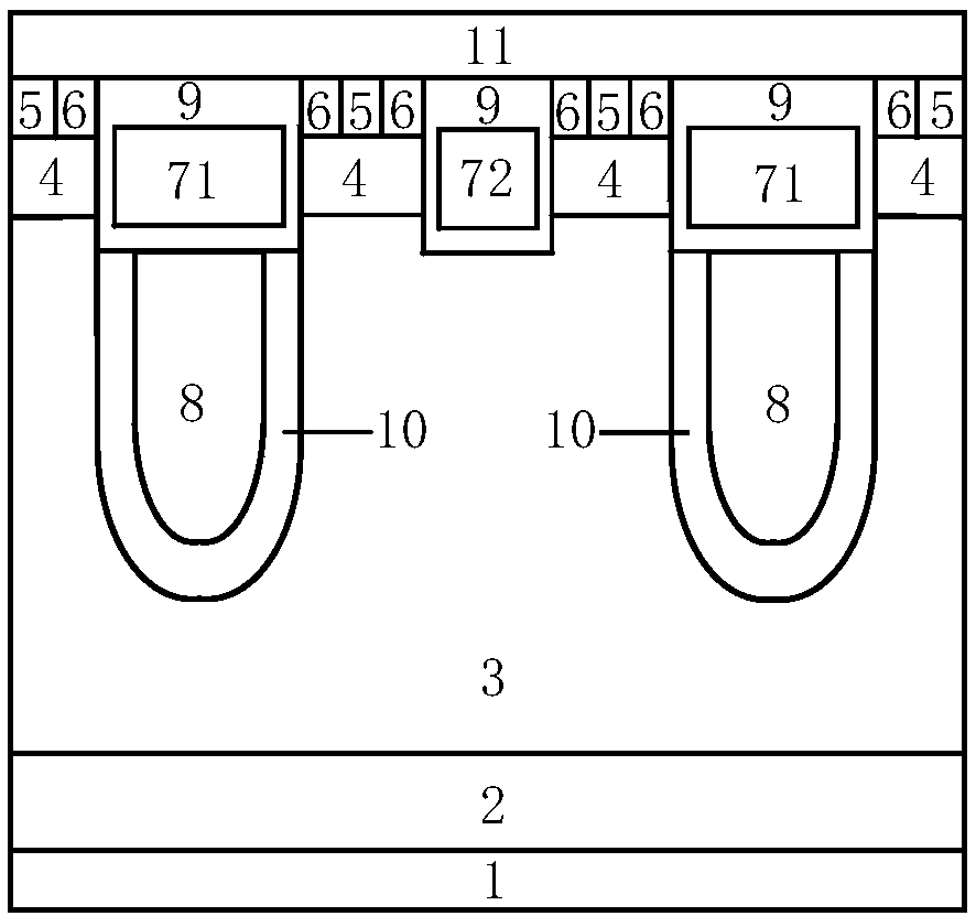
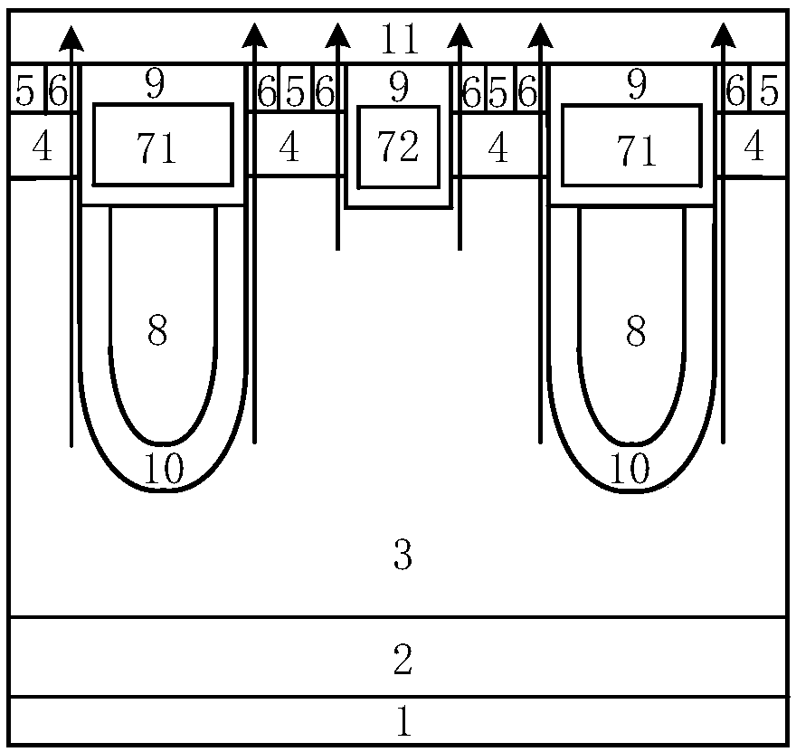
[0018] This embodiment provides a figure 1 The shielded gate power device shown includes a metallized drain 1, a first conductivity type semiconductor heavily doped substrate 2, a first conductivity type semiconductor drift region 3 and a metallization source 11 stacked sequentially from bottom to top; The upper layer of the first conductivity type semiconductor drift region 3 has a second conductivity type semiconductor body region 4; the upper layer of the second conductivity type semiconductor body region 4 has a second conductivity type semiconductor heavily doped contact region 5 and contacts with it The heavily doped source region 6 of the semiconductor of the first conductivity type has a first groove gate structure or a second groove gate structure with a depth smaller than the first groove gate structure between adjacent second conductivity type semiconductor body regions 4, the first groove gate structure structure and the second groove gate structure are alternately...

Embodiment 2

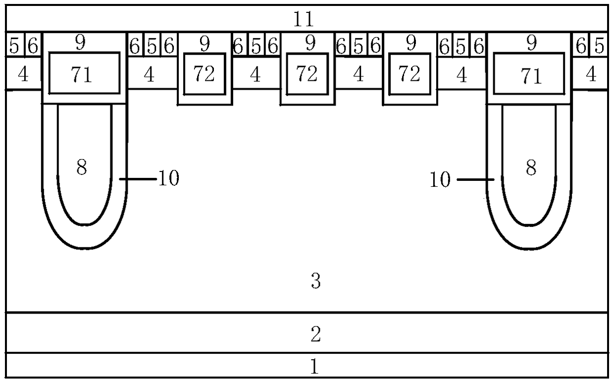
[0024] The difference between this embodiment of the present invention and Embodiment 1 is that there are multiple second groove gate structures between any two adjacent first groove gate structures, such as image 3 shown. Same as the first embodiment, the lateral width of the control gate electrode 71 is greater than the lateral width of the trench gate electrode 72 .


PUM


Abstract

The invention belongs to the technical field of power semiconductors, the invention aims at the problems that the cell density and the current capability of the conventional shielded gate power deviceare limited, A mask gate power device By arranging one or more TMOS cell structures between the conventional shielded gate cell structures, the channel density is increased under the same chip area,so that the cell density and current capability of the shielded gate MOS are improved while the gate drain capacitance is lower, the breakdown voltage is higher, and the on-resistance is lower.

Description

technical field [0001] The invention belongs to the technical field of power semiconductors, and in particular relates to a shielded gate power device. Background technique [0002] Power semiconductor devices are semiconductor devices for power processing, which combine microelectronics technology and power electronics technology to form the basis and core of power electronics technology. Power DMOS plays an important role in the field of power conversion because of its advantages such as fast switching speed, low loss, high input impedance, low driving power, and good frequency characteristics. Its development process is a process of continuously improving withstand voltage and reducing loss on the basis of maintaining its own advantages. The traditional VDMOS device is a planar structure using a double-diffusion process. It is the first power MOSFET successfully commercially applied and has played a key role in promoting the development of power MOSFETs. However, the exi...

Claims


Application Information

Patent Timeline
IPC IPC(8): H01L29/78H01L29/423
CPCH01L29/7813H01L29/4236H01L29/7831
Inventor 高巍何文静任敏蔡少峰李泽宏张金平张波
Owner UNIV OF ELECTRONIC SCI & TECH OF CHINA
Why Eureka
Try Eureka