

Infrared detector on basis of organic field-effect transistor and method for preparing infrared detector
An infrared detector and organic field technology, applied in the direction of organic semiconductor devices, semiconductor/solid-state device manufacturing, electric solid-state devices, etc., to achieve rich content, high-sensitivity and high-response detection, and enhance the effect of absorption
- Summary
- Abstract
- Description
- Claims
- Application Information
AI Technical Summary
Problems solved by technology
Method used
Image

Examples
Embodiment 1
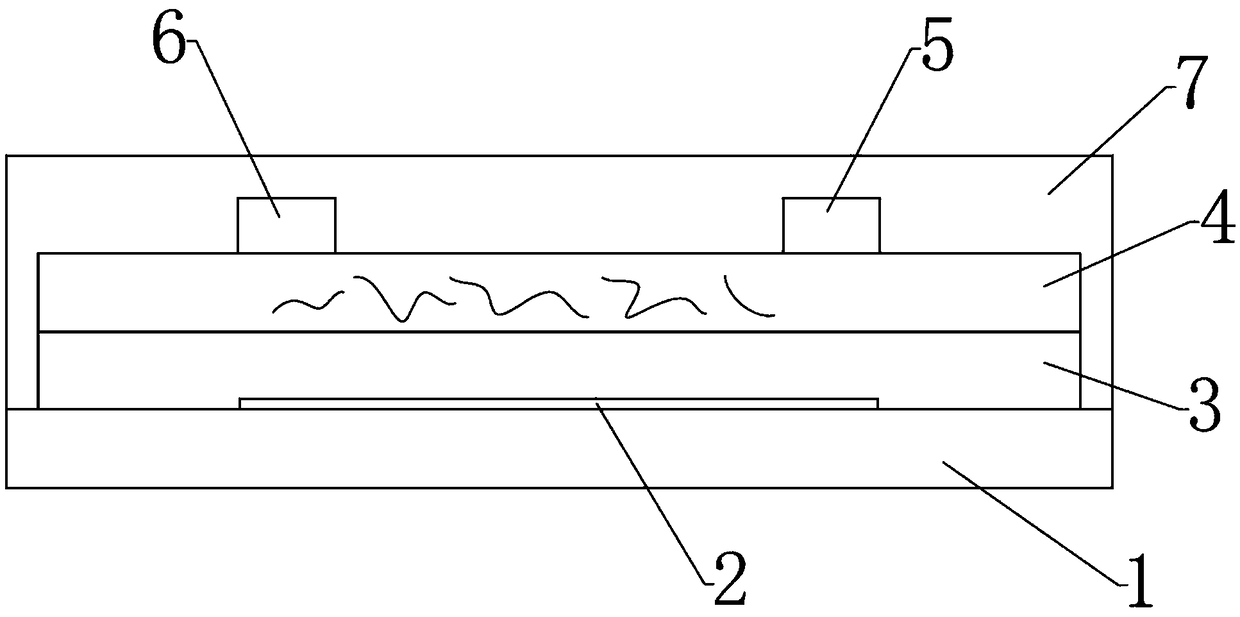
[0041] Such as figure 1 The bottom-gate top-contact structure is shown, and the material and thickness of each layer are as follows: the gate electrode, source electrode and drain electrode are all silver nanowires; the dielectric layer is made of silk fibroin with a thickness of 200nm; the organic semiconductor layer is made of carbon nanowires. The pipe is formed by mixing bamboo fibers (bamboo fiber mass fraction is 10%), and the thickness is 50nm; the shellac encapsulation layer has a thickness of 300nm. A field effect transistor infrared detector with high sensitivity and high stability can be realized by using the structure.
[0042] The preparation method of the present embodiment is as follows:
[0043] ① Clean the substrate with detergent, acetone solution, deionized water and isopropanol solution, and dry it with nitrogen after cleaning;
[0044] ② Prepare a 30nm thick silver nano wire grid electrode on the surface of the substrate;
[0045] ③The silk fibroin solu...
Embodiment 2
[0050] Such as figure 1 The bottom-gate top-contact structure is shown, and the material and thickness of each layer are as follows: the gate electrode, source electrode and drain electrode are all gold nanowires; the dielectric layer is made of silk fibroin with a thickness of 500nm; the organic semiconductor layer is 3- Hexylthiophene is mixed with bamboo fiber (the mass fraction of bamboo fiber is 5%), and the thickness is 30nm; the shellac encapsulation layer has a thickness of 200nm. A field effect transistor infrared detector with high sensitivity and high stability can be realized by using the structure.
[0051] The preparation method of the present embodiment is as follows:
[0052] ① Clean the substrate with detergent, acetone solution, deionized water and isopropanol solution, and dry it with nitrogen after cleaning;
[0053] ② Prepare a 30nm thick gold nano wire grid electrode on the surface of the substrate;
[0054] ③The silk fibroin solution with a concentrat...
Embodiment 3
[0059] Such as figure 1 The bottom-gate top-contact structure is shown, and the material and thickness of each layer are as follows: the gate electrode, source electrode and drain electrode are all iron nanowires; the dielectric layer is silk fibroin with a thickness of 600nm; the organic semiconductor layer is 6, 13-bis(triisopropylsilylethynyl) pentacene is mixed with bamboo fiber (the mass fraction of bamboo fiber is 8%), the thickness is 40nm, and the shellac encapsulation layer has a thickness of 200nm. A field effect transistor infrared detector with high sensitivity and high stability can be realized by using the structure.
[0060] The preparation method of the present embodiment is as follows:
[0061] ① Clean the substrate with detergent, acetone solution, deionized water and isopropanol solution, and dry it with nitrogen after cleaning;
[0062] ② Prepare a 30nm thick iron nano wire grid electrode on the surface of the substrate;
[0063] ③The silk fibroin soluti...
PUM
| Property | Measurement | Unit |
|---|---|---|
| Thickness | aaaaa | aaaaa |
| Thickness | aaaaa | aaaaa |
| Thickness | aaaaa | aaaaa |
Abstract
Description
Claims
Application Information