

Circulating nucleic acid detection kit based on microfluidic microbead array chip and application method thereof
A technology of microbead array chips and detection kits, which is applied in the determination/inspection of microorganisms, biochemical equipment and methods, etc., can solve the problems of long analysis period, low sensitivity, and large sample volume, and achieve independence from complex equipment , high sensitivity and simple operation
- Summary
- Abstract
- Description
- Claims
- Application Information
AI Technical Summary
Problems solved by technology
Method used
Image

Examples
Embodiment 1
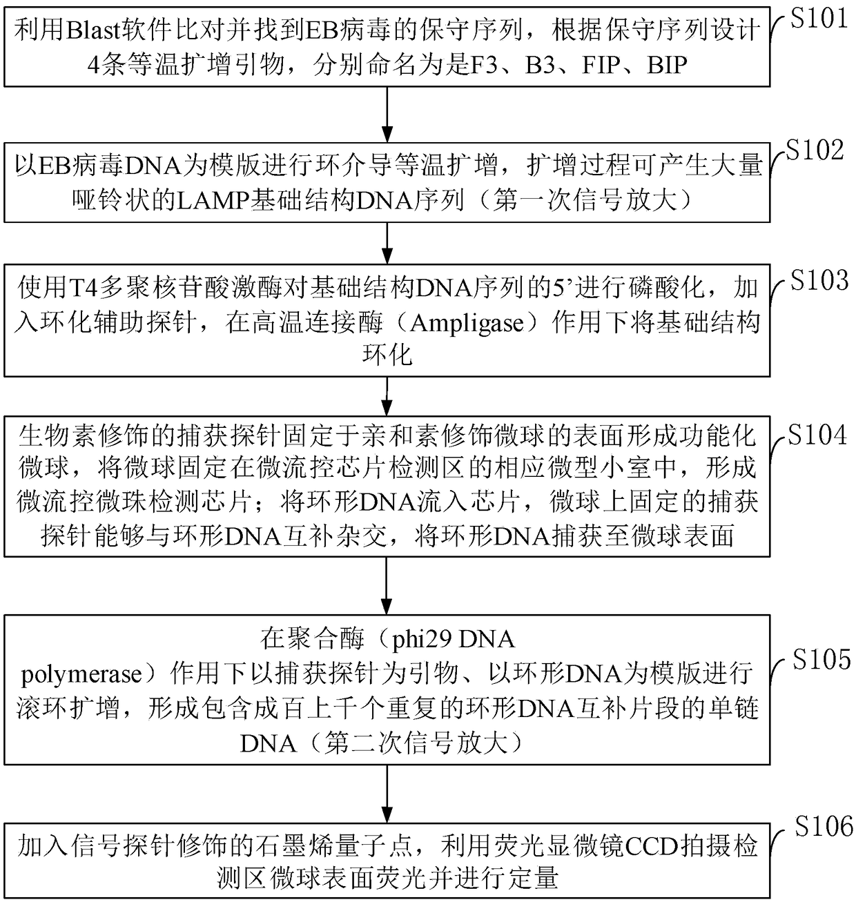
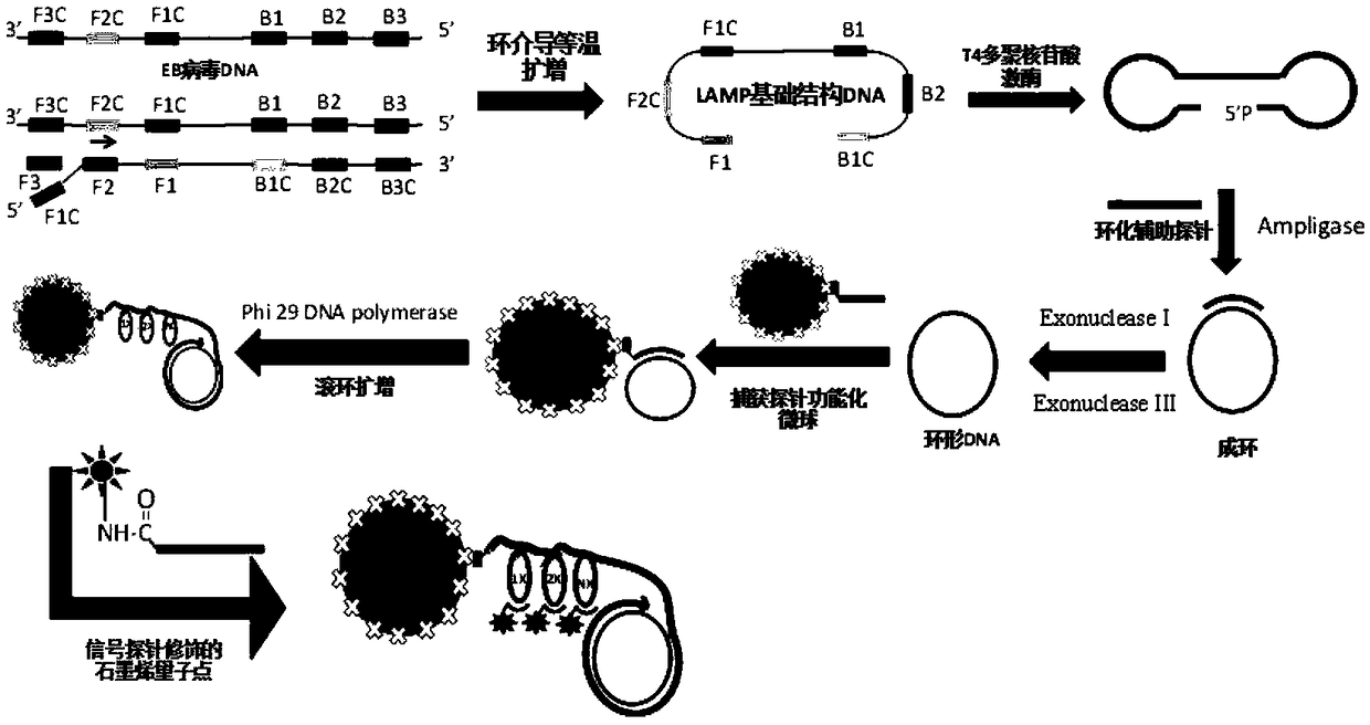
[0070] Prepare the detection kit according to the method described, the modified probes on the functionalized microspheres are as shown in the capture probes in Table 1, and the DNA probes for auxiliary basic structure DNA circularization are as shown in the circularization auxiliary probes in Table 1, The probes cross-linked with the aminated graphene quantum dots are shown in the signal probes in Table 1, and the loop-mediated isothermal amplification primers are shown in F3, B3, FIP, and BIP in Table 1, and the prepared Epstein-Barr virus DNA detection Reagent test kit.
[0071] Table 1 DNA sequence
[0072]
[0073]
[0074] BIP ATCACCTCTGATTCTGGCCCCCGCCGGGATGCTAATGTTCA loop-mediated isothermal amplification primers comprising B1C and B2SEQ ID NO:7.
[0075] The sequence of the basic structure of LAMP is SEQ ID NO: 8;
[0076] AGGGGCGGGTGGATTATCTGTTTGGGGGTGCAAGTTTTGGCTGGCCTGGGGGCCGTGGGGTCAACAGATAATCCACCCGCCCCTGGCGTGGAAGTTAATGTCCAGAGATCACCTCTGATTCTGGCCCCCAACGCCTCTGG...
Embodiment 2
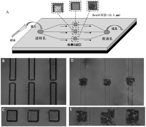
[0080] (1) Design and preparation of microfluidic chip and construction of detection chip
[0081] Firstly, the designed chip structure pattern is drawn by drawing software (CorelDRAW 9.0), and printed on Kodak film with a resolution of 2400dpi to prepare the photomask of the chip; then the pattern of the photomask is exposed by ultraviolet light Transfer to the PCB board covered with photoresist, and prepare the positive template of the chip on the exposed PCB board by chemical etching method; accurately weigh 12g polydimethylsiloxane prepolymer and 1.2g curing agent, stir Make it fully mixed for 5 minutes, remove the air bubbles in vacuum, and then spread it on the prepared chip positive template (thickness is about 1mm). The dimethylsiloxane (PDMS) sheet was peeled off from the positive template.
[0082] Such as figure 2 As shown, the schematic diagram of the structure of the microfluidic microbead array chip provided by the embodiment of the present invention and the s...
PUM
 Abstract
Description
Claims
Application Information