Large-size nano-porous BiVO4 photo-anode as well as preparation method and application thereof
A photoanode, three-electrode system technology, applied in the direction of electrode, electrode shape/type, energy input, etc., can solve problems such as low charge separation efficiency, increase film thickness, etc., to increase reaction sites, excellent stability, and improve photoelectricity. active effect
- Summary
- Abstract
- Description
- Claims
- Application Information
AI Technical Summary
Problems solved by technology
Method used
Image
Examples
Embodiment 1
[0046] A large-scale nanoporous BiVO 4 A photoanode and a preparation method thereof, comprising the steps of:
[0047] (1) Ultrasonic cleaning of fluorine-doped tin oxide (FTO) conductive glass:
[0048] First cut with a glass knife to obtain a conductive glass with a size of 7.5cm×10.0cm, then ultrasonically clean it with acetone, deionized water and ethanol for 30 minutes, and finally place it in an ethanol solvent.
[0049] (2) Deposit metal Bi:
[0050] First configure 250ml of 0.02mol / L bismuth nitrate solution, and deposit metal bismuth on the conductive glass by controlling the speed of glass immersion in the electrolyte and the amount of deposited charge during the electrodeposition process. The speed of glass immersion in the solution is 0.25cm / s, the deposition voltage is -1.0V Vs Ag / AgCl (reference electrode), and the deposition charge is 0.75C / cm 2 , to obtain the Bi / FTO precursor.
[0051] (3) Calcination to obtain Bi 2 o 3 / FTO precursor:
[0052] Put the...
Embodiment 2
[0058] This example prepares nanoporous BiVO with different Bi deposition charges 4 Photoanode, the preparation method is the same as that of Example 1, the difference is: the change of the charge amount of deposited metal Bi element in step (2): 0.25C / cm 2 , 0.50C / cm 2 , 1.0C / cm 2 .
Embodiment 3
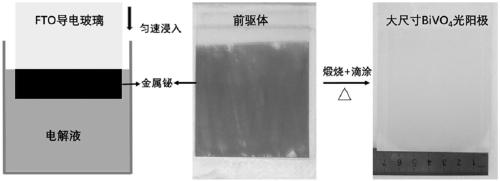
[0060] Schematic diagram of synthesizing a large-scale photoanode:
[0061] Examples 1 and 2 prepare large-sized nanoporous BiVO 4 The specific steps of the photoanode are as follows: figure 1 shown by figure 1 It can be seen that the photoanode preparation and synthesis method of the present invention has simple conditions, no pollution, and low cost. The test materials used are all conventional test materials in the field, and can be purchased through commercial channels.
PUM
| Property | Measurement | Unit |
|---|---|---|
| thickness | aaaaa | aaaaa |
| size | aaaaa | aaaaa |
| current density | aaaaa | aaaaa |
Abstract
Description
Claims
Application Information


