

Preparation method for transition-metal sulfide nanosheet sulfur vacancy
A technology of transition metals and nanosheets, applied in the field of defect control, can solve the problems of high equipment requirements, material damage, poor controllability and development, etc., and achieve the effect of simple preparation method, mild preparation method, precise preparation and regulation
- Summary
- Abstract
- Description
- Claims
- Application Information
AI Technical Summary
Problems solved by technology
Method used
Image

Examples
Embodiment 1
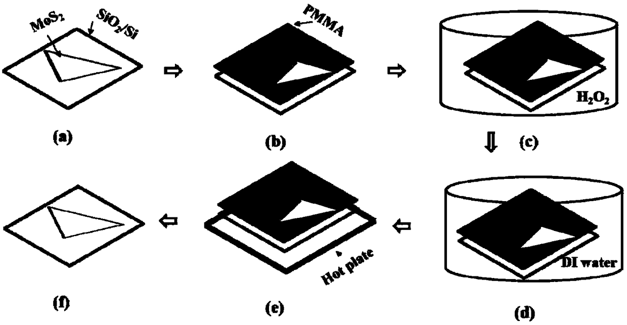
[0050] S1: Preparation of monolayer molybdenum disulfide on target substrate:
[0051] S1.1: Select molybdenum disulfide nanosheets with a thickness of 100 nanometers and transfer them to a silicon wafer to obtain a silicon wafer containing molybdenum disulfide nanosheets with a size of 30 microns.
[0052] S1.2: Spin-coat PMMA glue on the silicon wafer in S1, dry it at 120 °C for 2 min, put it in a 1:5 FH solution to etch away the silicon dioxide, and obtain a PMMA film with molybdenum disulfide.
[0053] S1.3: Use a clean silicon wafer to remove the PMMA film into deionized water, wash it repeatedly 15 times, and finally remove the cleaned PMMA film onto the marked target substrate, dry it at 120 °C for 10 min, and then remove it with acetone at 100 °C PMMA, to obtain monolayer molybdenum disulfide on the target substrate.
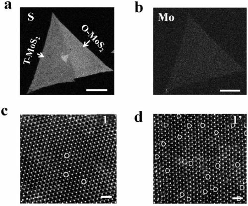
[0054] S1.4: Spin-coat PMMA onto the target substrate again, dry at 180 °C for 2 min, expose half of the single-layer triangular molybdenum disulfide a...
Embodiment 2
[0062] S1: Preparation of tungsten disulfide on the target substrate:
[0063] S1.1 Select tungsten disulfide nanosheets with a thickness of 20 nanometers and transfer them to a silicon wafer to obtain a silicon wafer containing tungsten disulfide nanosheets.
[0064] S1.2: Spin-coat PMMA glue on the silicon wafer containing tungsten disulfide nanosheets obtained in S1, dry at 100 °C for 6 minutes, put it into a 1:5 FH solution to etch away the silicon dioxide, and obtain a silicon wafer with tungsten disulfide PMMA films of nanosheets.
[0065] S1.3: Use a clean silicon wafer to remove the PMMA film into deionized water, wash it repeatedly 15 times, and finally remove the cleaned PMMA film onto the marked sapphire substrate, dry it at 120 °C for 10 min, and then remove it with acetone at 100 °C PMMA, to obtain a single layer of tungsten disulfide on the target substrate.
[0066] S1.4: Spin-coat PMMA onto the target substrate again, dry at 180 °C for 2 min, expose half of t...
Embodiment 3
[0073] S1: Preparation of monomolybdenum diselenide on the target substrate:
[0074] S1.1 Select molybdenum diselenide nanosheets with a thickness of 60 nanometers and transfer them to a silicon wafer to obtain a silicon wafer containing molybdenum diselenide nanosheets with a size of 80 microns.
[0075] S1.2: Spin-coat PMMA glue on the silicon wafer in S1, dry at 120 °C for 2 min, put it into a 1:5 FH solution to etch away the silicon dioxide, and obtain a PMMA film with molybdenum diselenide nanosheets .
[0076] S1.3: Use a clean silicon wafer to remove the PMMA film into deionized water, wash it repeatedly for 15 times, and finally remove the cleaned PMMA film onto the marked PET substrate, dry it at 120 °C for 10 min, and then remove it with acetone at 100 °C PMMA, to obtain a monolayer of molybdenum diselenide on a PET substrate.
[0077] S1.4: Spin-coat PMMA onto the target substrate again, dry at 180°C for 2 min, expose half of the molybdenum diselenide area using ...
PUM
| Property | Measurement | Unit |
|---|---|---|
| Size | aaaaa | aaaaa |
Abstract
Description
Claims
Application Information