Low-cost and efficient crystalline silicon solar cell module
A solar cell, low-cost technology, applied in the field of solar cells, can solve the problems of increased silicon wafer breakage rate, component cracking, chemical reagent consumption, and current loss, etc., to improve open circuit voltage and fill factor, shorten transportation distance, The effect of reducing compound loss
- Summary
- Abstract
- Description
- Claims
- Application Information
AI Technical Summary
Problems solved by technology
Method used
Image

Examples
Embodiment 1
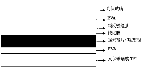
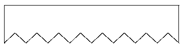
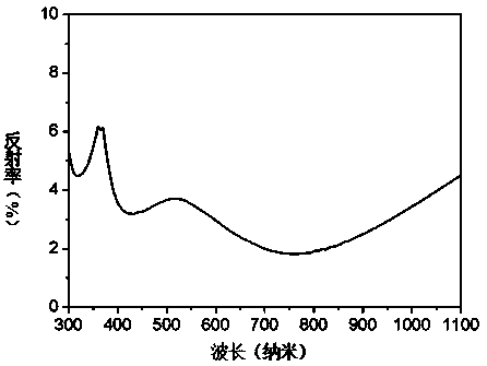
[0023] The emitter, passivation film, anti-reflection film, and electrode are sequentially prepared on the surface of the polished silicon wafer to form a cell, and then the cell is packaged with EVA and photovoltaic glass to form a component, where the passivation film is SiN x , with a thickness of 48 nm; the anti-reflection film has a two-layer structure, the first layer is close to the surface of the passivation film, its refractive index is 1.92, and its thickness is 47 nm. 1.62, the thickness is 59 nm; the refractive index of EVA is 1.48; the side of the photovoltaic glass facing the cell is an inverted pyramid structure, the bottom surface is a regular quadrilateral, and the apex angle of the cone is 54 o , with a height of 0.2 µm, a refractive index of 1.5, and a thickness of 2 mm. The average reflectance of the fabricated components is 3% in the wavelength range of 300-1100 nm.
Embodiment 2
[0025] Prepare the emitter, passivation film, anti-reflection film, and electrode on the surface of the polished silicon wafer in sequence to form a battery sheet, and then combine the battery sheet with EVA and photovoltaic glass to form a module, in which the passivation layer is SiO 2 , with a thickness of 30 nm; the anti-reflection film has a two-layer structure, the first layer next to the passivation layer has a refractive index of 2.3, and the thickness is 20 nm, and the second layer above the first layer has a refractive index of 2.0. The thickness is 74 nm; the refractive index of EVA is 1.5; the side of the photovoltaic glass facing the cell is an inverted pyramid structure, the bottom surface is a regular quadrilateral, and the apex angle of the cone is 54 o , the height is 0.2 µm, the refractive index of the glass is 1.51, and the average reflectance of the fabricated components is 4.8% in the wavelength range of 300-1100 nm.
Embodiment 3
[0027] Prepare the emitter, passivation film, anti-reflection film, and electrode on the surface of the polished silicon wafer in sequence to form a battery sheet, and then combine the battery sheet with EVA and photovoltaic glass to form a module, in which the passivation film is Al 2 o 3 , the thickness is 50 nm; the anti-reflection film has a two-layer structure, the first layer is next to the passivation layer, its refractive index is 2.37, and its thickness is 28 nm, and the second layer is above the first layer, its refractive index is 2.1, The thickness is 54 nm; the refractive index of EVA is 1.51; the side of the photovoltaic glass facing the cell is an inverted pyramid structure, the bottom surface is a regular quadrilateral, and the apex angle of the cone is 54 o , with a height of 0.2 µm, a refractive index of 1.52, and an average reflectance of 4% in the wavelength range of 300-1100 nm.
PUM
| Property | Measurement | Unit |
|---|---|---|
| Total thickness | aaaaa | aaaaa |
| Thickness | aaaaa | aaaaa |
| Thickness | aaaaa | aaaaa |
Abstract
Description
Claims
Application Information