Silicon wafer back-surface annealing and front-side coating integrated method and preparation method of battery piece

A battery chip and silicon chip technology, applied to circuits, electrical components, semiconductor devices, etc., can solve the problems of laser thermal shock on the back of the silicon chip, damage to the silicon matrix lattice structure, stress concentration, and loss of battery efficiency, etc., to improve solar energy. Effects of battery efficiency, reduction of cell fragmentation rate, and improvement of minority carrier life

Inactive Publication Date: 2019-04-12
HANWHA SOLARONE QIDONG
View PDF7 Cites 6 Cited by
  • Summary
  • Abstract
  • Description
  • Claims
  • Application Information

AI Technical Summary

Problems solved by technology

However, the slotting (opening) of the local passivation contact is mainly through high-energy laser bombardment of the passivation film on the back of the silicon wafer, which will cause severe laser the...

Method used


Image

  • Silicon wafer back-surface annealing and front-side coating integrated method and preparation method of battery piece
  • Silicon wafer back-surface annealing and front-side coating integrated method and preparation method of battery piece
  • Silicon wafer back-surface annealing and front-side coating integrated method and preparation method of battery piece

Examples


Embodiment 1

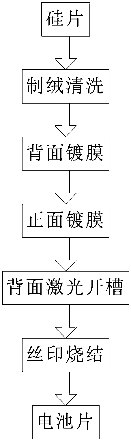
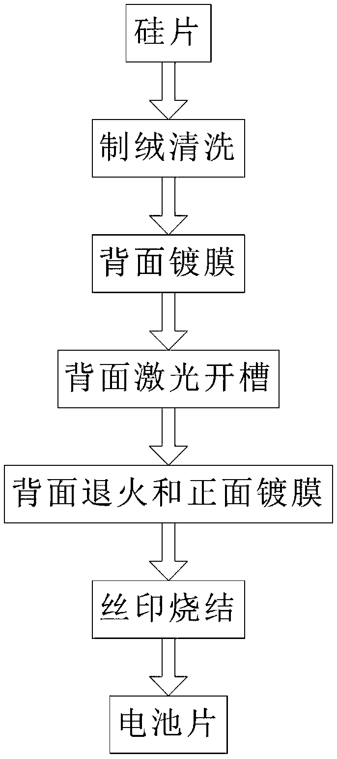
[0026] refer to Figures 2 to 3 , a method for preparing a battery sheet of the present embodiment, comprising the following steps:

[0027] Step S1: Prepare materials

[0028] Prepare single-polycrystalline silicon wafers with suitable resistivity, and perform texturing cleaning, back coating, etc. according to the battery process.

[0029] Step S2: Laser groove on the back

[0030] Put the silicon wafer that has undergone processes such as texture cleaning and back coating in step S1 into the laser equipment, set the laser percentage to 100% in the laser parameters, the laser frequency to 800kHz, and the laser pattern to be a regular hexagonal symmetrical pattern with a separation point of 500um , The size of the laser dot pattern is 155*155mm. After setting the appropriate laser parameters, the high-energy laser beam is used to bombard the film on the back of the silicon wafer to form the back groove (window) effect of removing the film and the molten silicon surface.

...

Embodiment 2

[0043] Embodiment 2 result and discussion

[0044] The detection of the battery sheet produced by using Example 1 and the battery sheet produced by the traditional process of Comparative Example 1, wherein Eta is the conversion efficiency, Uoc is the open circuit voltage, Isc is the short circuit current, FF is the fill factor, and Rs is Series resistance, Rsh is parallel resistance, IRev2 is reverse current, Breakage is screen fragmentation rate, the results are as follows:

[0045] Table 1 Test results

[0046]

[0047] In Example 1, the back annealing and the front coating are integrated, and the lattice defects and thermal stress damage are repaired by annealing, so as to improve battery efficiency and reduce hidden crack fragments. From the electrical performance test results in Table 1, it can be concluded that the gain in photoelectric conversion efficiency of the battery in Example 1 comes from the improvement of Uoc, the main reason is that after laser damage anneal...


PUM


Abstract

The invention discloses a silicon wafer back-surface annealing and front-side coating integrated method, which comprises the following steps of carrying out laser grooving on the back surface of a silicon wafer by utilizing laser equipment, placing the silicon wafer subjected to laser grooving into a deposition device, introducing reaction gas SiH4 and NH3 and N2 into the deposition cavity of thedeposition device for deposition so as to coat the front surface of the silicon wafer. According to the silicon wafer back surface annealing and front surface coating integrated method, the laser grooving is carried out before the front surface coating process, and the back annealing is carried out by utilizing the medium-high-temperature oxygen-free environment in the PECVD process, and meanwhile, the front-surface film coating can be synchronously completed, no extra annealing process is added; the thermal shock, thermal damage and crystal lattice defects caused by the high-energy laser grooving on the back surface can be recovered and restored; and the composite rate of the damaged surface of the silicon wafer after laser is further reduced, and the method also can be used for carryingout hydrogen passivation on the position of the back grooving (window opening), so that the minority carrier lifetime of the silicon wafer damaged by the laser is prolonged, and the efficiency of thesolar cell is further improved.

Description

technical field [0001] The invention relates to the technical field of solar cell manufacturing, in particular to a method for integrating back annealing and front coating of a silicon wafer and a method for preparing a solar cell including the integrated method. Background technique [0002] With the continuous development of photovoltaic technology, crystalline silicon solar cells have developed rapidly as a clean energy product that converts solar energy into electrical energy. [0003] The matching optimization of passivation and contact can continuously improve the efficiency of crystalline silicon solar cells. The aluminum back field has developed from the entire surface of the aluminum-silicon contact to the currently widely used PERC partially passivated aluminum-silicon contact, which reduces the recombination rate on the back of the silicon wafer and reduces the Minority carrier recombination improves battery efficiency. However, the slotting (opening) of the loca...

Claims


Application Information

Patent Timeline
IPC IPC(8): H01L31/18
CPCH01L31/18H01L31/1864Y02P70/50
Inventor 李懋鸿费存勇赵福祥崔钟亨张金花
Owner HANWHA SOLARONE QIDONG
Why Eureka
Try Eureka