JCD integrated device based on P type epitaxy and preparation method thereof

A technology for integrating devices and device areas, which is applied in semiconductor/solid-state device manufacturing, electrical solid-state devices, semiconductor devices, etc., and can solve problems such as integration barriers, complex JFET device manufacturing processes, and large chip leakage currents.

Active Publication Date: 2019-04-23
UNIV OF ELECTRONICS SCI & TECH OF CHINA
View PDF2 Cites 5 Cited by
  • Summary
  • Abstract
  • Description
  • Claims
  • Application Information

AI Technical Summary

Problems solved by technology

[0002]For more than 40 years, semiconductor technology has been shrinking the chip feature size along the route of Moore's Law. However, semiconductor technology has developed to a bottleneck: with the increasing line width The smaller the size, the manufacturing cost increases exponentially; and as the line width approaches the nanometer scale, the quantum effect becomes more and more obvious, and the leakage current of the chip becomes larger and larger
However, the integration technology of JFET devices still has many problems such as compatibility and poor performance of JFET devices.
Due to the particularity of the double-gate structu...

Method used


Image

  • JCD integrated device based on P type epitaxy and preparation method thereof
  • JCD integrated device based on P type epitaxy and preparation method thereof
  • JCD integrated device based on P type epitaxy and preparation method thereof

Examples


Embodiment 1

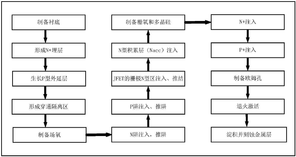
[0073] This embodiment provides a method for manufacturing a JCD integrated device based on P-type epitaxy, such as figure 1 Shown is a schematic diagram of the manufacturing process flow of the integrated device of the present invention, which specifically includes the following main process steps:

[0074] Step 1: Prepare the substrate;

[0075] preparation The crystal-oriented boron-doped silicon substrate is used as the P-type substrate 1; the resistivity of the P-type substrate 1 in this embodiment is 40-50Ω·cm, and the substrate thickness is 550-750um;

[0076] Step 2: Form N+ buried layer;

[0077] The CMOS device area, PJFET device area and well resistance area of ​​the P-type silicon substrate 1 prepared in step 1 are etched with NBL (NBuried Layer) plate, and phosphorus is ion implanted without high temperature push junction. On the P-type silicon substrate 1 N+ buried layers 201~203 are respectively formed on the surface; in this embodiment, the ion implantation energy is...


PUM


Abstract

The invention relates to a JCD integrated device based on a P type epitaxy and a preparation method thereof, and belongs to the technical field of power semiconductor integration. The preparation method mainly comprises the following process steps of preparing a substrate; forming an N+ buried layer; growing a P type epitaxial layer; forming a penetration isolation region; preparing field oxygen;performing N trap injection and trap pushing; performing P trap injection and trap pushing; performing JFET grid electrode N type region injection and junction pushing; preparing gate oxygen and polycrystalline silicon; performing N+ injection; performing P+ injection; preparing ohm holes; performing annealing activation; performing deposition and etching a metal layer; integrating PJFET, CMOS, nLDMOS (and/or without) Poly resistors, Poly diodes, Poly capacitors and trap resistors into the same chip. The JCD integrated device provided by the invention has the advantages that the high-low voltage device compatibility is good; the isolation effect is good; the mask templates are few; the JFET has the advantages of high precision simulation features, great input impedance, high-speed, good anti-radiation features and the like; the integration of the low-voltage JEFT devices with high-voltage control DMOS parts and low-voltage logic CMOS parts is realized; the JCD integrated device can beapplied to the process design of the power source management IC, protection circuits and integrated operation amplifiers.

Description

Technical field [0001] The invention belongs to the technical field of power semiconductor integration, and specifically relates to a P-type epitaxy-based JCD integrated device and a preparation method thereof. Background technique [0002] For more than 40 years, semiconductor technology has been shrinking the feature size of chips along the route of Moore’s Law. However, the current semiconductor technology has developed to a bottleneck: as the line width becomes smaller and smaller, the manufacturing cost increases exponentially; and as the line width approaches At the nanometer scale, the quantum effect is becoming more and more obvious, and the leakage current of the chip is also increasing. Therefore, the development of semiconductor technology must consider the "post-Moore era" issue. In 2005, the international technology roadmap for semiconductors (ITRS) put forward the concept of more than Moore. Power semiconductor devices and power integration technology play a very ...

Claims


Application Information

Patent Timeline
IPC IPC(8): H01L27/07H01L21/8232H01L21/8234H01L21/8238
CPCH01L21/8232H01L21/8234H01L21/8238H01L27/0705
Inventor 李泽宏蒲小庆杨尚翰王志明任敏张金平高巍张波
Owner UNIV OF ELECTRONICS SCI & TECH OF CHINA
Why Eureka
Try Eureka