

JCD integrated device integrated with VDMOS and preparation method thereof
A technology for integrating devices and device areas, which is applied in semiconductor/solid-state device manufacturing, electrical solid-state devices, semiconductor devices, etc., and can solve the problems of complex JFET device manufacturing process, rising manufacturing cost, and poor performance of compatible JFET devices.
- Summary
- Abstract
- Description
- Claims
- Application Information
AI Technical Summary
Problems solved by technology
Method used
Image

Examples
Embodiment 1
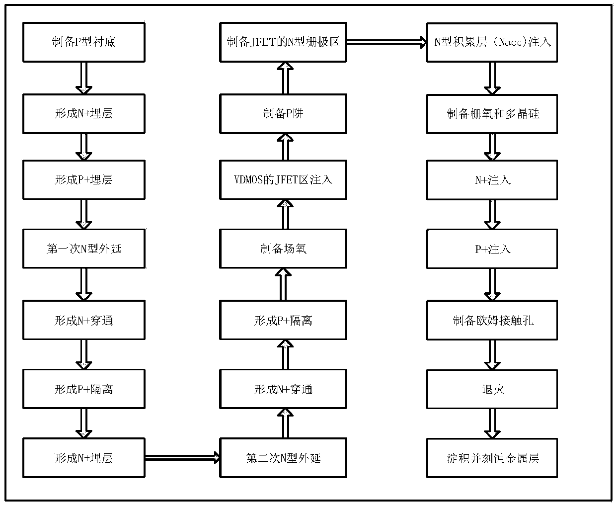
[0080] This embodiment provides a method for manufacturing a JCD integrated device based on N-type epitaxy, such as figure 1 Shown is a schematic diagram of the manufacturing process flow of the integrated device of the present invention, which specifically includes the following main process steps:
[0081] Step 1: Prepare the substrate;
[0082] preparation A boron-doped silicon substrate with crystal orientation is used as the P-type substrate 1; in this embodiment, the P-type substrate 1 has a resistivity of 30-50Ω·cm and a substrate thickness of 550-750um;
[0083] Step 2: Form N+ buried layer;
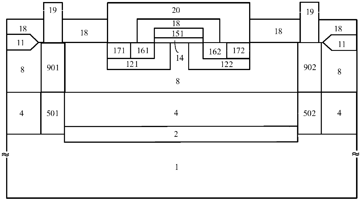
[0084] On the surface of the high-voltage VDMOS device area of the P-type silicon substrate 1 prepared in step 1, the NBL1N Buried Layer plate is used for etching, and phosphorus is ion-implanted without high-temperature push to form an N+ buried layer 201; in this embodiment, the ion implantation energy 60KeV, ion implantation dose is 1e15~5e15cm -2 ;
[0085] Step 3: Form P+ buried ...
PUM
 Abstract
Description
Claims
Application Information