Full-transition metal nitride current collector/electrode supercapacitor and preparation method thereof

A supercapacitor, transition metal technology, applied in the manufacture of hybrid/electric double-layer capacitors, hybrid capacitor electrodes, hybrid capacitor current collectors, etc., can solve the problem of frequency response (poor rate characteristics, etc.) The effect of many, the process is simple and easy to implement

Active Publication Date: 2019-05-03
DALIAN UNIV OF TECH
View PDF4 Cites 8 Cited by
  • Summary
  • Abstract
  • Description
  • Claims
  • Application Information

AI Technical Summary

Problems solved by technology

In recent years, French scholars have reported that TiN and VN films with high resistivity (ρ>1000μΩ.cm) porous structure have high specific capacitance values ​​comparable to carbon-based, graphene-based, and transition metal oxide electrode materials, but in In the prepared supercapacitor, the above-mentioned film is used as both an electrode material and a current collector at the same time. Due to the high resistivity of the film, it also leads to the problem of poor frequency response (magnification) characteristics.

Method used


Image

  • Full-transition metal nitride current collector/electrode supercapacitor and preparation method thereof
  • Full-transition metal nitride current collector/electrode supercapacitor and preparation method thereof
  • Full-transition metal nitride current collector/electrode supercapacitor and preparation method thereof

Examples


Embodiment example 1

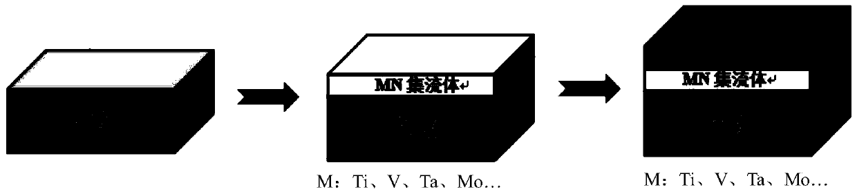
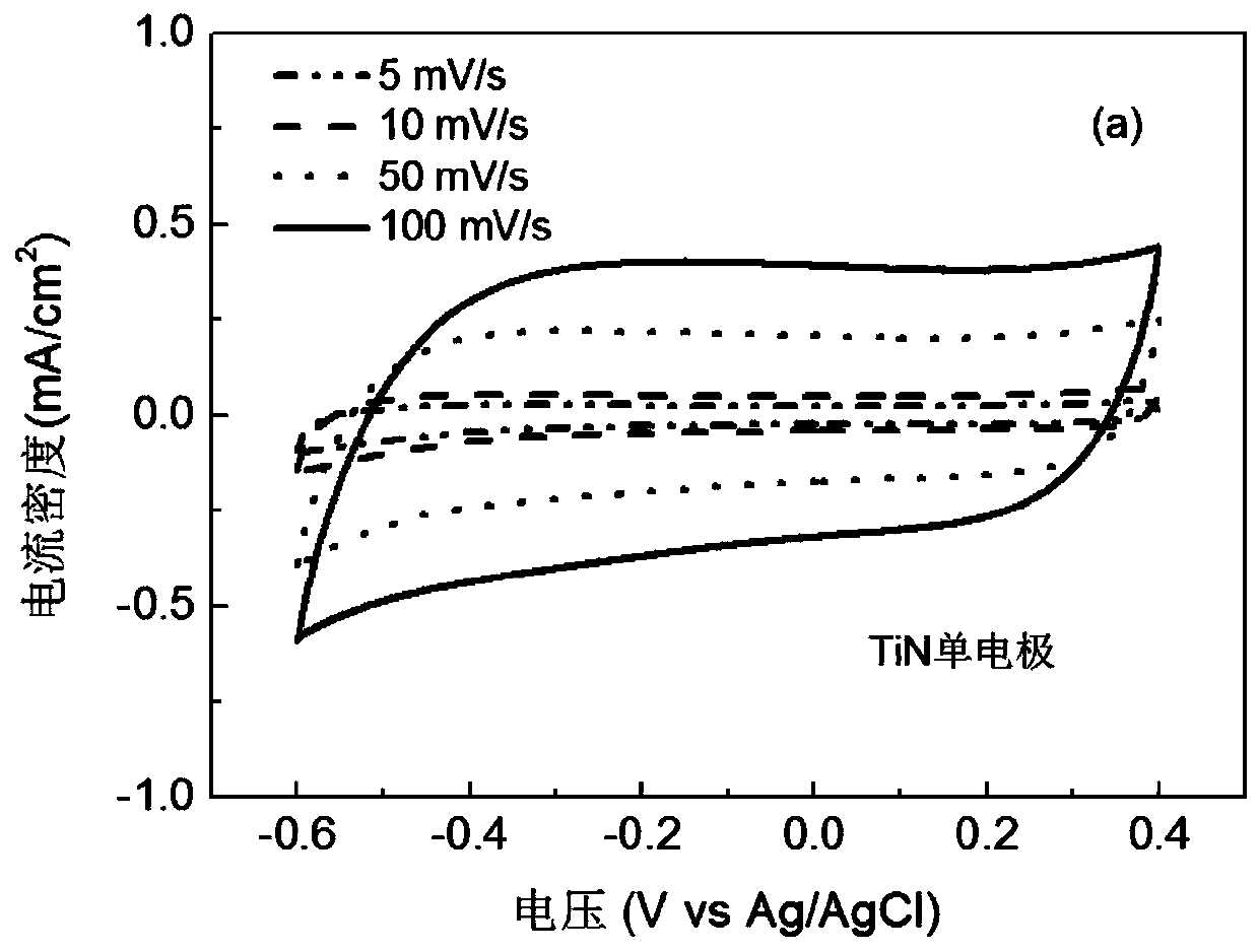
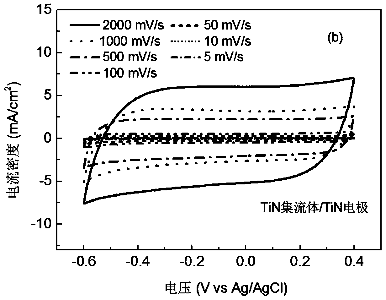
[0031] In this embodiment, a single crystal silicon substrate is selected as the substrate, and the semiconductor industry standard RCA cleaning process is used for cleaning. DC reactive magnetron sputtering is adopted, the target material is titanium metal, the base distance of the target is 20cm, Ar:N 2 =10:1sccm, sputtering power: 100W, substrate temperature: 400°C, working pressure: 0.2Pa, substrate bias voltage: -50V, sputtering time: 10min, first deposit a layer with a thickness of 38nm, and a resistivity of 108μΩ·cm , the surface is smooth and dense TiN thin film is used as the current collector material, and then the distance between the target and the base is 20cm, Ar:N 2 =10:1sccm, sputtering power: 100W, substrate temperature: 400°C, working pressure: 0.4Pa, sputtering time: grow a layer of thickness 240nm under the conditions of 30min, resistivity 2800μΩ·cm, loose and porous TiN film as electrode material. Using a three-electrode test system, the working electrod...

Embodiment example 2

[0033] In this embodiment, a single crystal silicon substrate is selected as the substrate, and the semiconductor industry standard RCA cleaning process is used for cleaning. DC reactive magnetron sputtering is adopted, the target material is titanium metal, the base distance of the target is 40cm, Ar:N 2 =20:1sccm, sputtering power: 200W, substrate temperature: 300°C, working pressure: 0.2Pa, substrate bias: -50V, sputtering time: 10min, deposit a layer with a thickness of 30nm first, and a resistivity of 128μΩ·cm , the surface is smooth and dense TiN thin film is used as the current collector material, and then the distance between the target and the base is 20cm, Ar:N 2 =10:1sccm, sputtering power: 100W, substrate temperature: 400°C, working pressure: 0.4Pa, sputtering time: grow a layer of thickness 240nm under the conditions of 30min, resistivity 2800μΩ·cm, loose and porous TiN film as electrode material. Using a three-electrode test system, the working electrode is TiN...

Embodiment example 3

[0035] In this embodiment, a single crystal silicon substrate is selected as the substrate, and the semiconductor industry standard RCA cleaning process is used for cleaning. Using radio frequency reactive magnetron sputtering, the target material is vanadium metal, the target base distance is 50cm, Ar:N 2 =20:1sccm, sputtering power: 150W, substrate temperature: 200°C, working pressure: 0.6Pa, substrate bias: -150V, sputtering time: 20min, first deposit a layer with a thickness of 79nm and a resistivity of 188μΩ·cm , the surface is smooth and dense VN thin film as the current collector material, and then the distance between the target and the base is 50cm, Ar:N 2 =20:1sccm, sputtering power: 150W, substrate temperature: 200°C, working pressure: 0.6Pa, sputtering time: grow a layer of thickness 300nm under the condition of 40min, resistivity 3600μΩ·cm, loose and porous VN film as electrode material. Using a three-electrode test system, the working electrode is VN, the count...


PUM

PropertyMeasurementUnit
thicknessaaaaaaaaaa
electrical resistivityaaaaaaaaaa

Abstract

The invention discloses a full-transition metal nitride current collector/electrode supercapacitor and a preparation method thereof, and belongs to the technical field of new energy materials and devices. Firstly, impurities on the surface of a substrate material are removed through cleaning. Secondly, a layer of high-density and high-conductivity transition metal nitride film is deposited on thesurface of the substrate to serve as an electron transport current collector material. Thirdly, a layer of loose, porous and low-conductivity transition metal nitride film is directly and continuouslygrown on the current collector by regulating and controlling deposition process parameters to serve as an electrode material. According to the invention, the current collector and the electrode are both transition metal nitrides which grow continuously. The performance of the material is cut by simply changing film deposition process parameters. The preparation method is simple, convenient and feasible in process, low in cost, multiple in thin film deposition technology selection types and high in process applicability. The problems of layered cracking and large contact resistance caused by poor adhesion force, lattice mismatch and thermal expansion coefficient difference between a heterogeneous current collector and an electrode material are solved. The power density, the thermal stability and the long-term service reliability of the super capacitor are greatly improved.

Description

technical field [0001] The invention belongs to the technical field of new energy materials and devices, and relates to a full-transition metal nitride collector / electrode supercapacitor and a preparation method thereof. Background technique [0002] Supercapacitors have significant advantages such as high energy and power density, long charge-discharge cycle life, wide operating temperature range, maintenance-free, environmentally friendly and pollution-free, and have attracted widespread attention as a new type of green energy storage method. In recent years, the research and popularization of various sensor systems in the wireless Internet of Things, as well as wearable and implantable medical devices have developed rapidly. And the urgent need for full monolithic integration with other electronic components. Supercapacitors are mainly composed of electrode materials, current collectors and electrolytes, among which electrode materials and current collectors are importan...

Claims


Application Information

Patent Timeline
Patent Type & Authority Applications(China)
IPC IPC(8): H01G11/30H01G11/68H01G11/26H01G11/84H01G11/86
CPCY02E60/13
Inventor 周大雨孙纳纳杨旭马晓倩
Owner DALIAN UNIV OF TECH
Why Eureka
Try Eureka