Novel plasma enhanced chemical vapor deposition (PECVD) coating technology

A process and new technology, applied in the field of new PECVD coating process, can solve the problems of increasing the surface recombination rate, surface damage, reducing the short-circuit current of the battery, etc., to reduce the recombination center, increase the electron-hole pair, and improve the short-circuit current.

Inactive Publication Date: 2019-05-07
JETION SOLAR HLDG
View PDF8 Cites 1 Cited by
  • Summary
  • Abstract
  • Description
  • Claims
  • Application Information

AI Technical Summary

Problems solved by technology

This coating method, because the plasma bombards the surface of the silicon wafer, will cause serious surface damage and form more surface defects, which greatly increases the surface recombination rate and reduces the short-circuit current of the battery.

Method used


Image

  • Novel plasma enhanced chemical vapor deposition (PECVD) coating technology

Examples


Embodiment 1

[0042] PECVD coating is performed on the surface of polysilicon, and the process settings are as follows:

[0043] (1) Polysilicon feeding into the furnace: the temperature is 450°C, the nitrogen flow rate is 5000 sccm, and the time is 250s;

[0044] (2) Heating up in the furnace: the temperature is 450°C, the nitrogen flow rate is 5000 sccm, and the time is 550s;

[0045] (3) Ammonia purging: the temperature is controlled at 425° C., and the flow rate of ammonia gas of 5500 sccm is introduced for 65 seconds;

[0046] (4) Vacuum leak detection: the temperature is controlled at 420°C, and the furnace tube is pumped with a vacuum pump. The pressure reaches 100mTorr within 200s, and is maintained for 30-120s. Observe whether the pressure exceeds 100mTorr;

[0047] (5) Pre-deposition: input ammonia gas 5000sccm, silane 550sccm, turn on the radio frequency generator, the radio frequency power is 5000w, set the time for 15s, then turn off the radio frequency, and the gas input stop...

Embodiment 2

[0056] (1) Density test of PECVD film on silicon wafer

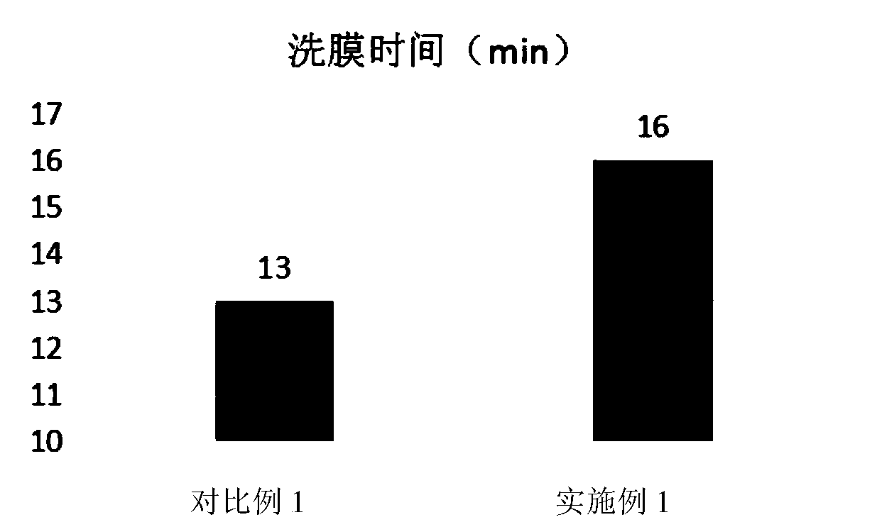
[0057] The compactness of the PECVD film is judged by the pickling time, randomly select 25 silicon wafers produced in Comparative Example 1 and 25 silicon wafers produced in Example 1, and put them into a 15% hydrofluoric acid solution together. In the utensil, count the time when the PECVD film is soaked. Such as figure 1 , the film washing time of embodiment 1 is 3 minutes more than the film washing time of comparative example 1, illustrates that the PECVD film compactness of embodiment 1 is higher than the PECVD film of comparative example 1, adopts technology of the present invention to coat PECVD film to silicon chip , the density of its PECVD film is better.

[0058] (2) Electrical performance test of the battery sheet prepared in Comparative Example 1 and Example 1

[0059] The silicon wafers produced in Comparative Example 1 and Example 1 are sent to the screen section, and are dried by the screen printing ba...


PUM


Abstract

The invention relates to the field of crystalline silicon surface coating, in particular to a novel plasma enhanced chemical vapor deposition (PECVD) coating technology. The technology comprises the steps that crystalline silicon is placed into a furnace and heated, and the temperature is stabilized; ammonia gas is introduced for purging; vacuumizing for leakage detection is performed; pre-deposition is performed; chemical reaction gas is injected, and radio frequency ionization is performed; vacuumizing is performed; gas is injected; annealing is performed; and the coated crystalline siliconis taken out of the furnace. According to battery pieces prepared through silicon wafers coated by means of the coating technology provided by the invention, bombardment damage on the surfaces of thesilicon wafers is repaired, the number of dangling bonds on the surfaces of the silicon wafers is decreased, the number of recombination centers is decreased, the recombination rate of electrons is decreased, the number of electron hole pairs used for outputting current is increased, the short-circuit current of the battery pieces is increased, the efficiency of the battery pieces is improved, andthe competitiveness in the industry is greatly enhanced.

Description

technical field [0001] The invention relates to the technical field of crystalline silicon surface coating, in particular to a novel PECVD (PlasmaEnhanced Chemical Vapor Deposition) coating process. Background technique [0002] Solar energy is an inexhaustible renewable energy source for human beings, and it is also a clean energy source that does not produce any environmental pollution. At present, crystalline silicon solar cells occupy 90% of the market share in the entire solar cell industry, and its cost and price have been declining on a large scale. With the continuous development of the solar industry, the pursuit of high-efficiency cells has become an inevitable trend. [0003] The production steps of crystalline silicon solar cells include: cleaning of silicon wafer surface and preparation of light-trapping structure, diffusion to prepare PN junction, back etching to remove phospho-silicate glass, PECVD to prepare anti-reflection film, screen printing back electrod...

Claims


Application Information

Patent Timeline
Patent Type & Authority Applications(China)
IPC IPC(8): C23C16/02C23C16/513C23C16/56H01L31/18
CPCY02P70/50
Inventor 钱小芳杨冬生孙明晶
Owner JETION SOLAR HLDG
Why Eureka
Try Eureka