High-reliability NIP structure mesa type photodiode and manufacturing method thereof

A technology of photodiode and manufacturing method, applied in sustainable manufacturing/processing, circuits, electrical components, etc., can solve problems such as complex surface protection, achieve the effect of suppressing leakage current and edge breakdown, and improving reliability

Active Publication Date: 2019-05-07
THE 44TH INST OF CHINA ELECTRONICS TECH GROUP CORP
View PDF11 Cites 6 Cited by
  • Summary
  • Abstract
  • Description
  • Claims
  • Application Information

AI Technical Summary

Problems solved by technology

[0005] In order to solve the problems existing in the prior art and improve the reliability of the mesa chip, the present invention proposes a highly reliable NIP structure mesa photodiode. The P-type layer of the diode is placed at the lowest part and buried deep inside the material, which can avoid problems such as leakage and complicated surface protection

Method used


Image

  • High-reliability NIP structure mesa type photodiode and manufacturing method thereof
  • High-reliability NIP structure mesa type photodiode and manufacturing method thereof
  • High-reliability NIP structure mesa type photodiode and manufacturing method thereof

Examples


Embodiment 1

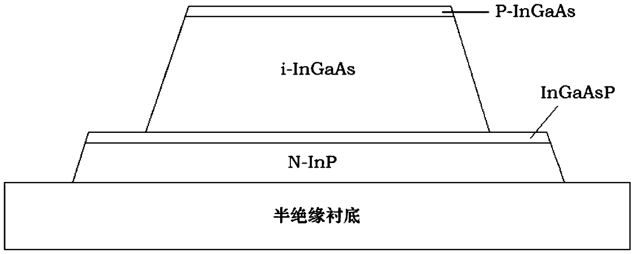
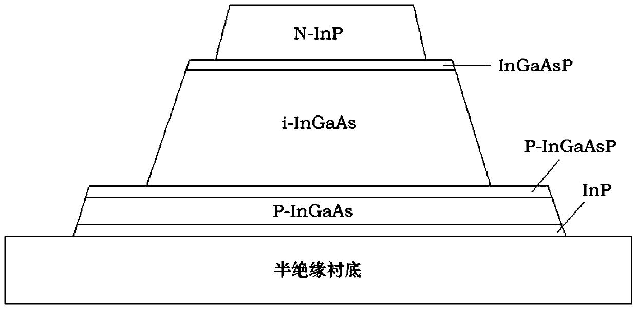
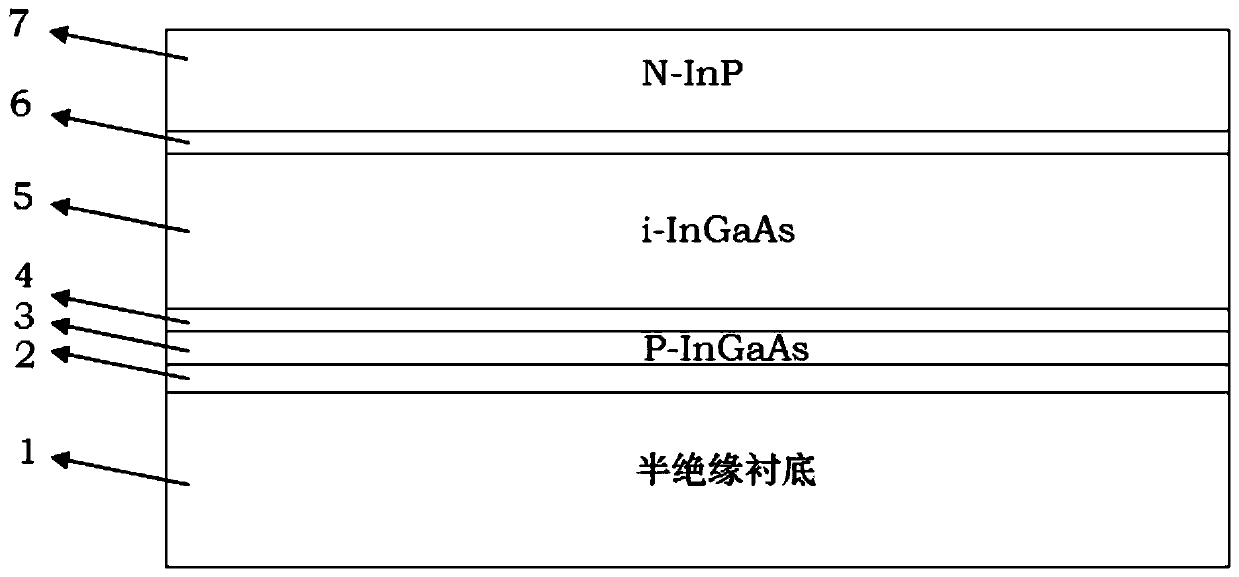
[0034] As a specific embodiment, the present invention will be described in detail below in conjunction with the accompanying drawings and process flow. In this embodiment, the chip structure epitaxial material is grown on a semi-insulating substrate by metal organic chemical vapor deposition (MOCVD) or molecular beam epitaxy (MBE). Bottom 1, that is, on the InP substrate, the structure can be as follows figure 2 and image 3 As shown, in order:

[0035] 1) buffer layer 2

[0036] A weak n-type indium phosphide (InP) buffer layer is used, and its carrier concentration is 1×10 15 cm -3 , with a thickness of 0.1-0.5 μm;

[0037] 2) P-type contact layer 3

[0038] Use P-type InGaAs contact layer, doped with carbon, carrier concentration ≥ 1×10 18 cm -3 , with a thickness of 0.1-0.5 μm.

[0039] 3) Barrier layer 4

[0040] P-type indium gallium arsenide phosphide (InGaAsP) barrier layer, doping concentration ≥ 1×10 18 cm -3 , and its growth thickness is 0.01-0.2 micron...

Embodiment 2

[0048] The manufacturing process of the present embodiment includes the following steps:

[0049] 1) Deposition on epitaxial material by plasma enhanced chemical vapor deposition (PECVD) A silicon nitride (SiNx) dielectric film is used to define the mesa region of the first layer through a photolithography process.

[0050]2) The first layer of mesa is defined by dry etching or wet etching. Dry etching can use inductively coupled plasma etching (ICP) or reactive ion etching (RIE); wet etching can use For acid series, acid oxygen series, and bromine series etching solutions, the etching or etching depth must reach the InGaAsP gradient layer.

[0051] 3) Using the photoresist as a mask to define the mesa region of the second layer through a photolithography process.

[0052] 4) The second mesa is defined by dry etching or wet etching. Dry etching can be inductively coupled plasma etching (ICP) or reactive ion etching (RIE); wet etching can use For acid series, acid oxygen ...


PUM


Abstract

The present invention relates to the field of semiconductor photodiodes, and in particular to a high reliability NIP structure mesa type photodiode and a manufacturing method thereof. The photodiode comprises a semi-insulating substrate on which a buffer layer, a contact layer, an absorption layer, a gradient and a blocking are grown; the structure comprises a three-layer mesa chip structure, themesa surface is covered with a passivation layer, an N electrode is introduced from an N-type mesa, a P electrode is introduced from a P-type mesa, so that the P electrode and the N electrode form a coplanar electrode. The NIP structure photodiode is employed to put the P-type layer at the lowest portion and allow the P-type layer to be deeply buried in the material so as to avoid the problem of leakage and complex surface protection; and the geometric design of the three-layer mesa is employed to effectively limit a built-in electric field at the center of the body, minimize the edge electricfield around the mesa and inhibit the leakage current of the edge of the mesa and the edge breakdown so as to improve the reliability of the diode chip.

Description

technical field [0001] The invention relates to the field of semiconductor photodiodes, in particular to a highly reliable NIP structure mesa photodiode and a manufacturing method. The invention can effectively improve the reliability of the mesa chip. Background technique [0002] In fiber optic communication systems, photodiodes are used to convert information-carrying optical signals into information-carrying electrical signals, so that subsequent circuits can process the information. Depending on the way the PN junction is formed, it can be divided into planar photodiodes and mesa photodiodes. The PN junction of the planar photodiode is buried inside the epitaxial layer, which has good reliability, but the PN junction has a lateral expansion effect, and the high-speed performance is poor. The PN junction of the mesa photodiode is exposed in the air, and the reliability is poor, but the high-speed performance is good. [0003] As the high-speed optical fiber communicat...

Claims


Application Information

Patent Timeline
Patent Type & Authority Applications(China)
IPC IPC(8): H01L31/105H01L31/0352H01L31/18
CPCY02P70/50
Inventor 王立黄晓峰崔大健高新江莫才平迟殿鑫樊鹏张承
Owner THE 44TH INST OF CHINA ELECTRONICS TECH GROUP CORP
Why Eureka
Try Eureka