Preparation method of large-size single crystal beta-gallium oxide nanobelt structure

A gallium nitride nanotechnology, gallium oxide technology, applied in chemical instruments and methods, nanotechnology, nanotechnology, etc., can solve the problems of uncontrollable growth direction, different crystal phases of nanomaterials, etc., to achieve universality and good repeatability , Reduce the time required, the effect of simple process

Active Publication Date: 2019-06-14
纳微朗科技(深圳)有限公司
View PDF2 Cites 4 Cited by
  • Summary
  • Abstract
  • Description
  • Claims
  • Application Information

AI Technical Summary

Problems solved by technology

[0004] The present invention aims to solve the problems of different crystal phases and uncontrollable growth directions of existing nanomaterials, and provides a simple process, controllable thickness, and good repeatability to prepare large-size single crystal β- Gallium oxide nanoribbon method

Method used


Image

  • Preparation method of large-size single crystal beta-gallium oxide nanobelt structure
  • Preparation method of large-size single crystal beta-gallium oxide nanobelt structure
  • Preparation method of large-size single crystal beta-gallium oxide nanobelt structure

Examples


example 1

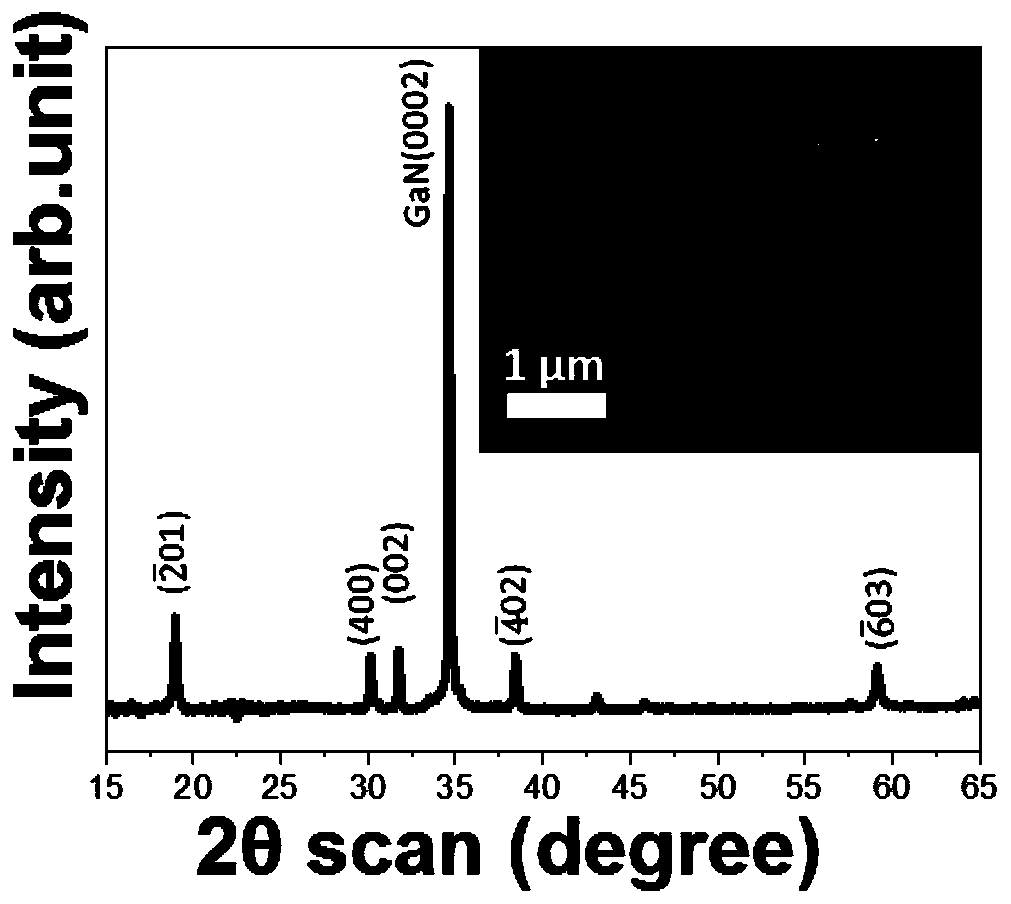
[0058] Example 1: Preparation of (-201) single crystal β-gallium oxide nanowires.

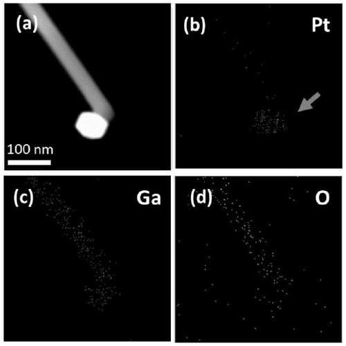
[0059] (1) A thin layer of platinum is plated on the gallium nitride film:

[0060] Before the gallium oxide nanostructure is grown on the gallium nitride film, an 8nm-thick platinum thin layer is evaporated on the gallium nitride surface.

[0061] (2) Place the gallium nitride film into the chemical vapor deposition equipment, and form catalytic particles on the surface of the gallium nitride film by annealing:

[0062] Put the gallium nitride film in step (1) into the CVD chamber, and the pressure in the chamber of the chemical vapor deposition equipment is stabilized at 1.01×10 5 Pa, flow argon gas with a flow rate of 300 sccm, raise the temperature to 800°C, and maintain the temperature for annealing for 30min.

[0063] (3) Annealing in a low-oxygen environment to form gallium nitride nanoseed crystals wrapped with catalytic particles on the film:

[0064] Inject 400 sccm of argon gas fo...

Embodiment 2

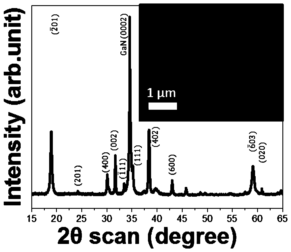
[0068] Embodiment 2: Single crystal β-gallium oxide nanobelt and device.

[0069] (1) A thin layer of platinum is plated on the gallium nitride film:

[0070] Before the gallium oxide nanostructure is grown on the gallium nitride film, 4nm, 6nm, and 8nm thick platinum thin layers are respectively evaporated on the surface of the gallium nitride.

[0071] (2) Place the gallium nitride film into the chemical vapor deposition equipment, and form platinum particles on the surface of the gallium nitride film by annealing:

[0072] Put the gallium nitride film in step (1) into the CVD chamber, and the pressure in the chamber of the chemical vapor deposition equipment is stabilized at 1.01×10 5 Pa, flow argon gas with a flow rate of 100 sccm, raise the temperature to 500°C, and maintain the temperature for annealing for 60min.

[0073] (3) Annealing in a low-oxygen environment to form gallium nitride nanoseed crystals wrapped with platinum particles on the film:

[0074] Evacuate ...

Embodiment 3

[0079] Embodiment 3: Single crystal β-gallium oxide nanobelt and device.

[0080] (1) A thin layer of platinum is plated on the gallium nitride film:

[0081] Before the gallium oxide nanostructure is grown on the gallium nitride film, a platinum thin layer with a thickness of 8 nm is evaporated on the surface of the gallium nitride.

[0082] (2) Place the gallium nitride film into the chemical vapor deposition equipment, and form platinum particles on the surface of the gallium nitride film by annealing:

[0083] Put the gallium nitride film in step (1) into the CVD chamber, and the pressure in the chamber of the chemical vapor deposition equipment is stabilized at 1.01×10 5 Pa, flow argon gas with a flow rate of 100 sccm, raise the temperature to 500°C, and maintain the temperature for annealing for 60min.

[0084] (3) Annealing in a low-oxygen environment to form gallium nitride nanoseed crystals wrapped with platinum particles on the film:

[0085] Evacuate the air pres...


PUM

PropertyMeasurementUnit
lengthaaaaaaaaaa
widthaaaaaaaaaa
thicknessaaaaaaaaaa

Abstract

The invention belongs to the technical field of semiconductor materials, and particularly relates to a large-size single crystal beta-gallium oxide nanobelt structure and a preparation method thereof.The preparation method comprises: firstly plating a catalytic thin layer on the surface of a gallium nitride film; placing into a chemical vapor deposition device, and thermally annealing the galliumnitride thin film covered with the catalytic thin layer; growing a {-201} single crystal gallium oxide nanowire on the gallium nitride film under a less oxygen condition by a thermal oxidation growthmethod; by utilizing the growth condition of rich gallium / less oxygen, selectively growing in a side direction on the side face of the nanowire to obtain the large-sized single crystal beta-gallium oxide nanobelt. The preparation method has the advantages of simple process and good universality and repeatability, can overcome the disadvantage of different crystal phases of a catalytically grown gallium oxide nano material, the grown gallium oxide nanobelt controllable in thickness, is high in yield, and the can be stably transferred on various substrates for the preparation of various novel gallium oxide based devices.

Description

technical field [0001] The invention belongs to the technical field of semiconductor materials, and in particular relates to a preparation method of a large-size single crystal β-gallium oxide nanobelt. Background technique [0002] β-Gallium oxide material, as a direct bandgap wide bandgap semiconductor, has an ultra-wide bandgap with a bandgap of 4.9eV, a high breakdown electric field and a Barrega value, high thermal / chemical stability, and High transparency of visible light and other advantages. Therefore, with the development of semiconductor material technology, gallium oxide materials have received extensive attention and research due to their excellent physical, chemical, electrical and other properties. [0003] Compared with bulk materials, nanomaterials (0-dimensional quantum dots, 1-dimensional nanowires and 2-dimensional materials) have special properties such as larger body surface area, quantum size confinement effect, quantum tunneling effect, and unusual P...

Claims


Application Information

Patent Timeline
Patent Type & Authority Applications(China)
IPC IPC(8): C30B25/02C30B29/16C30B29/64C30B33/02C23C16/40B82Y30/00B82Y40/00
Inventor 方志来蒋卓汛吴征远闫春辉张国旗
Owner 纳微朗科技(深圳)有限公司
Why Eureka
Try Eureka