Application of two-dimensional palladium selenide nano film for detection of broadband polarized light signals
A palladium nano, polarized light technology, applied in the field of photoelectric detection, can solve the problems of limited application of two-dimensional materials, poor chemical stability, and inability to exist stably, and achieve the effects of significant light response, accurate detection, and fast response speed.
- Summary
- Abstract
- Description
- Claims
- Application Information
AI Technical Summary
Problems solved by technology
Method used
Image
Examples
Embodiment 1
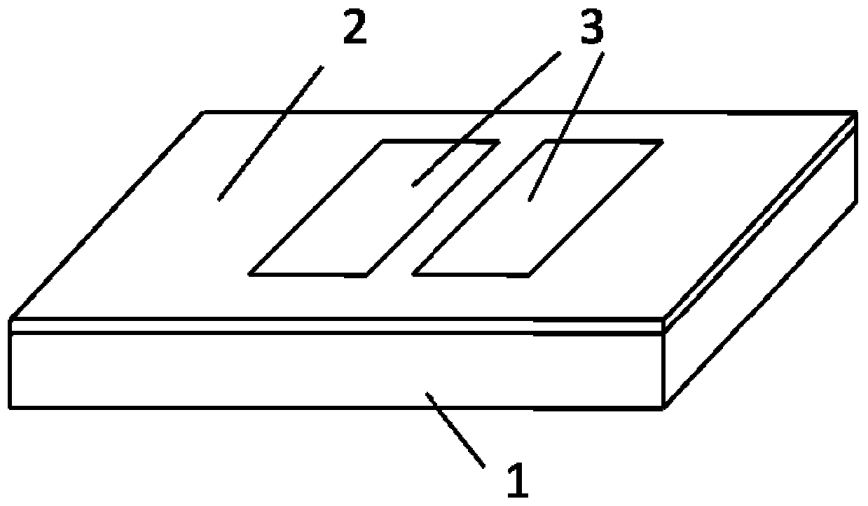
[0034] Such as image 3 As shown, in this embodiment, a two-dimensional palladium diselenide nanofilm grown on a silicon oxide substrate is used to directly construct a polarization-sensitive photoconductive photodetector. Specifically, a pair of metal electrodes 3 in ohmic contact with the two-dimensional palladium diselenide nano-film 2 is prepared on the two-dimensional palladium diselenide nano-film 2, and a gold electrode with a thickness of 50 nanometers is used in this embodiment. Tests have shown that if Figure 4As shown, the photodetector of this embodiment has a response sensitivity of 5.1 to polarized light at 650 nm.
Embodiment 2
[0036] Such as Figure 5 As shown, this embodiment is based on the heterojunction of two-dimensional palladium diselenide nano-film and germanium to construct a polarization-sensitive heterojunction photodetector. The specific method is: first transfer the two-dimensional palladium diselenide nano-film to On the germanium substrate: Then prepare a 100-nanometer-thick silver electrode on the surface of the two-dimensional palladium diselenide film by thermal evaporation as the first metal electrode, and prepare a 100-nanometer-thick indium-gallium alloy electrode on the surface of the germanium substrate as the second metal electrode, That is, the preparation of the polarization-sensitive heterojunction photodetector is completed. Tests have shown that if Figure 6 As shown, the photodetector of this embodiment has good photoresponse to ultraviolet, visible and infrared light. In addition, the response sensitivity of the device to polarized light at 980 nm is 7.9, such as F...
Embodiment 3
[0038] Such as Figure 8 As shown, this embodiment is based on the heterojunction of two-dimensional palladium diselenide nano film and silicon nanowire array to construct a polarization-sensitive heterojunction photodetector. The specific method is: firstly, two-dimensional palladium diselenide nano The film is transferred to the surface of the silicon nanowire array: then by thermal evaporation, gold with a thickness of 80 nm is deposited on the surface of the two-dimensional palladium diselenide film as the first metal electrode, and silver with a thickness of 100 nm is prepared on the silicon nanowire array as the first metal electrode. The second metal electrode is to complete the preparation of the polarization-sensitive heterojunction photodetector. Wherein, the silicon nanowire array is prepared by metal-assisted chemical etching. Tests have shown that if Figure 9 As shown, the response sensitivity of the photodetector of this embodiment to the polarized light of 15...
PUM
| Property | Measurement | Unit |
|---|---|---|
| Thickness | aaaaa | aaaaa |
Abstract
Description
Claims
Application Information


