Schottky diode and preparation method thereof

A Schottky diode and electrode technology, applied in semiconductor/solid-state device manufacturing, electrical components, circuits, etc., can solve problems such as high cost, high technical difficulty, and inability to Schottky diodes, and achieve improved stability and low turn-on Voltage, effect of high reverse breakdown voltage

Active Publication Date: 2019-06-21
珠海镓未来科技有限公司
View PDF7 Cites 15 Cited by
  • Summary
  • Abstract
  • Description
  • Claims
  • Application Information

AI Technical Summary

Problems solved by technology

[0003] Research on gallium oxide is still in its infancy. Although experiments have shown that the test value of the breakdown electric field of gallium oxide devices has exceeded the theoretical value of gallium nitride and silicon carbide, the electrical characteristics of gallium oxide devices under current process conditions are compared with other There is still a certain gap in the third generation of semiconductor devices
Due to the deep energy level of the gallium oxide acceptor and the hole self-confinement effect, it is difficult to dope traditional p-type acceptor elements into gallium oxide to form a p-type material. PN junction is usually accompanied by high technical difficulty and high cost
This largely limits the use of gallium oxide materials to make Schottky diodes, that is, it is impossible to use gallium oxide materials to make high-performance Schottky diodes

Method used


Image

  • Schottky diode and preparation method thereof
  • Schottky diode and preparation method thereof
  • Schottky diode and preparation method thereof

Examples


Embodiment

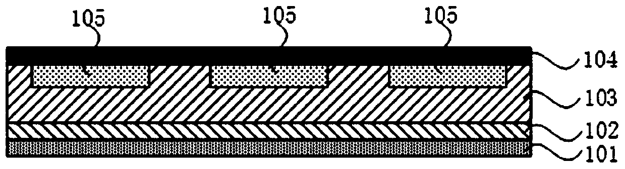
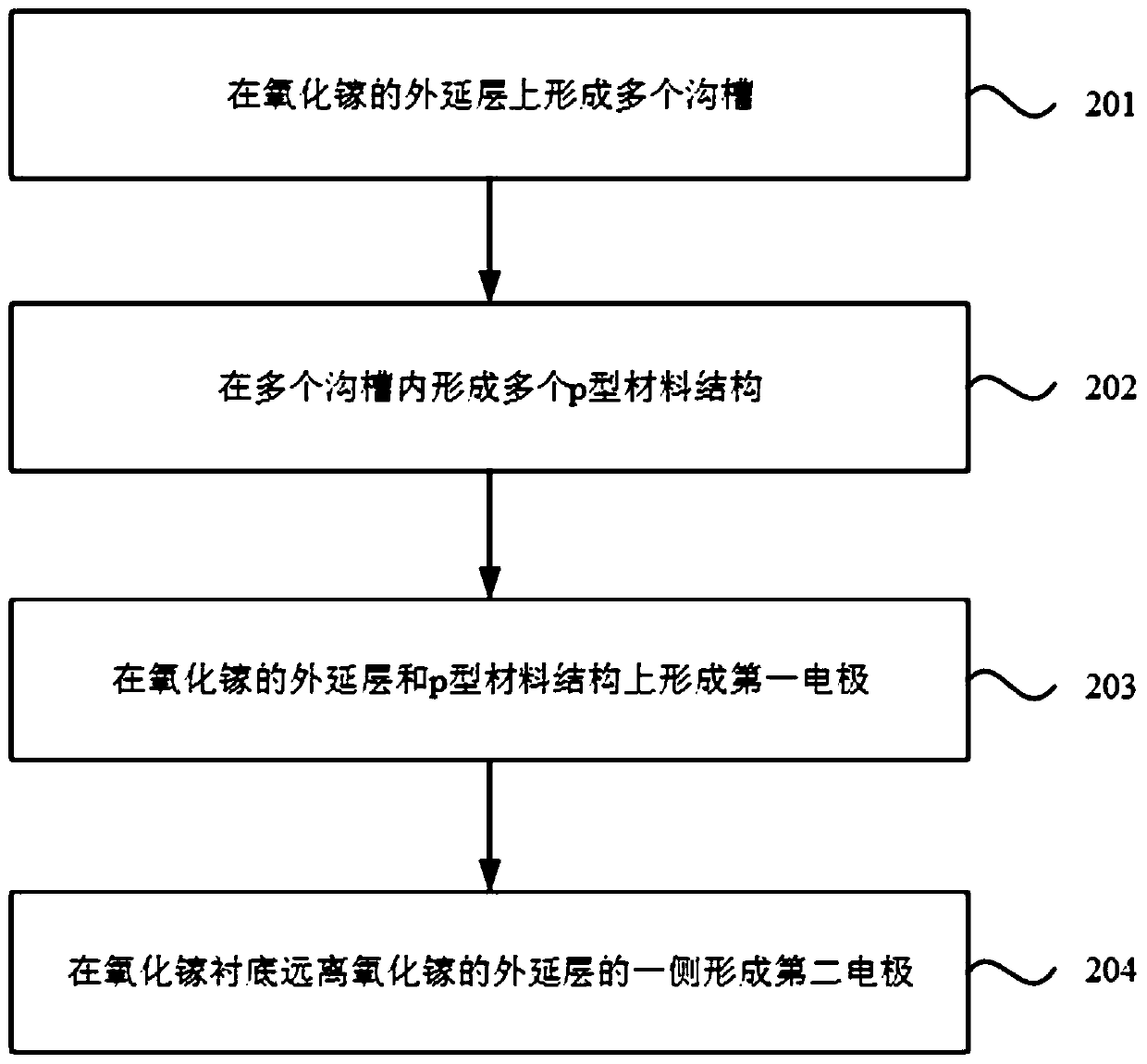
[0037] refer to figure 1 , figure 1 A schematic structural diagram of a Schottky diode provided by an embodiment of the present invention, the Schottky diode includes a gallium oxide substrate 102;

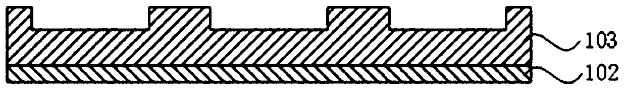
[0038] a gallium oxide epitaxial layer 103 on a gallium oxide substrate 102, wherein a plurality of grooves are provided on a side of the gallium oxide epitaxial layer 103 away from the gallium oxide substrate 102;

[0039] a p-type material structure 105 located in the plurality of trenches;

[0040] a first electrode 104 covering the p-type material structure 105 and the gallium oxide epitaxial layer 103;

[0041] The second electrode 101 is located on the side of the gallium oxide substrate 102 away from the gallium oxide epitaxial layer 103 .

[0042] Specifically, the gallium oxide substrate 102 is n-type highly doped (n+) gallium oxide, and the gallium oxide epitaxial layer 103 is n-type low-doped (n-); the gap between the second electrode 101 and the gallium oxide substr...


PUM

PropertyMeasurementUnit
thicknessaaaaaaaaaa
temperatureaaaaaaaaaa

Abstract

The invention discloses a Schottky diode and a preparation method thereof. The Schottky diode comprises a gallium oxide substrate, a gallium oxide epitaxial layer on the gallium oxide substrate, a plurality of P-type material structures, a first electrode and a second electrode; a plurality of trenches are formed in the side, away from the gallium oxide substrate, of the gallium oxide epitaxial layer; the plurality of p-type material structures are located in the plurality of trenches; he first electrode covers the p-type material structures and the gallium oxide epitaxial layer; and the second electrode is located on the side, away from the gallium oxide epitaxial layer, of gallium oxide substrate. A heterogeneous PN junction structure is formed between the p-type material structures andthe gallium oxide epitaxial layer, thereby solving the problems of high technical difficulty and high cost accompanying with the manufacturing of high-performance Schottky diodes as the gallium oxidematerials are difficult to form p-type doping materials; and meanwhile, the manufactured Schotty diode has relatively low turn-on voltage at high voltage and high current, and has relatively high reverse breakdown voltage, thereby improving the working stability of the Schottky diode.

Description

technical field [0001] Embodiments of the present invention relate to semiconductor technology, and in particular to a Schottky diode and a manufacturing method thereof. Background technique [0002] Gallium oxide is a wide bandgap semiconductor material. The bandgap width of β-Ga2O3 is about 4.85eV, its critical breakdown electric field is as high as 8MV / cm, and n-type doping is controllable, radiation resistant, high melting point, very suitable for making High voltage power electronic devices. Its applications include power electronic devices, radio frequency electronic devices, ultraviolet detectors, gas sensors, etc., and have broad application prospects in solid-state lighting, communications, consumer electronics, new energy vehicles, and smart grids. Gallium oxide has better high-voltage resistance characteristics than third-generation semiconductor materials such as silicon carbide. Its Baliga figure of merit (BFOM) is about 4 times higher than that of gallium nitr...

Claims


Application Information

Patent Timeline
Patent Type & Authority Applications(China)
IPC IPC(8): H01L29/872H01L21/329H01L29/06
CPCH01L29/06H01L29/872
Inventor 于洪宇曾凡明
Owner 珠海镓未来科技有限公司
Why Eureka
Try Eureka