
Electronic component and method for manufacturing electronic component

A technology of electronic components and electrodes, which is applied in the field of electronic components and electronic component manufacturing, can solve problems such as inability to fully realize miniaturization, achieve the effects of avoiding dimensional changes, ensuring connection reliability, and improving electrical reliability

Active Publication Date: 2019-07-02
TOPPAN INC
View PDF7 Cites 4 Cited by
  • Summary
  • Abstract
  • Description
  • Claims
  • Application Information

AI Technical Summary

Problems solved by technology

However, there is also a demand for further miniaturization, and it is not possible to achieve sufficient miniaturization only by miniaturization of the above-mentioned small passive components and high-density mounting with respect to the substrate surface

Method used


Image

  • Electronic component and method for manufacturing electronic component
  • Electronic component and method for manufacturing electronic component
  • Electronic component and method for manufacturing electronic component

Examples


Embodiment 1

[0086] Such as figure 2 As shown, a glass substrate 100 (OA-10G manufactured by Nippon Denki Glass Co., Ltd., thickness: 0.5 mm, linear thermal expansion coefficient: 3 ppm / K) was prepared. Next, if image 3As shown, a through-hole 101 with a top diameter of 80 um and a bottom diameter of 60 um among the diameters of the through-hole 101 was formed by using a picosecond laser processing machine. and, if Figure 4 As shown, on the front and back of the glass substrate 100 , a 50 nm titanium film and a 300 nm copper film are formed by sputtering as the seed metal layer 102 . Furthermore, an electroless nickel plating layer with a thickness of 0.1 μm was formed for the purpose of increasing the size of the seed metal layer 102 in the through hole 101 . As above, the seed metal layer 102 made of titanium, copper, and nickel was formed.

[0087] Then, if Figure 5 As shown, a photosensitive dry film resist having a thickness of 25 μm was provided on the seed metal layer 102 b...


PUM

PropertyMeasurementUnit
diameteraaaaaaaaaa
diameteraaaaaaaaaa
coating thicknessaaaaaaaaaa

Abstract

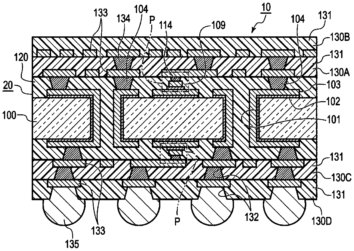
An electronic component according to the present invention is provided with: a glass base material (100) having a through-hole (101) formed so as to pass through both surfaces thereof; an insulating resin layer (120) that is stacked on each of both surfaces of the glass base material (100) and that has a copper-plated layer (103) formed in the interior thereof; and a capacitor (109) having a lowerelectrode (110) formed on the copper-plated layer (103), a dielectric layer (111) formed so as to be stacked on the lower electrode (110), and an upper electrode (112) formed so as to be stacked on the dielectric layer (111). A region of the upper electrode (112), said region being along the surface of the copper-plated layer (103), is formed so as to be smaller than a region of the dielectric layer (111), said region being along the surface of the copper-plated layer (103), and a region of the lower electrode (110), said region being along the surface of the copper-plated layer (103). This provides a glass core substrate having a thin-film capacitor with a highly reliable MIM structure and also achieves a compact size, a small thickness, and high reliability.

Description

technical field [0001] The present invention relates to an electronic component and a method of manufacturing the electronic component, and in particular, to a structure incorporating a capacitor having a highly reliable structure that is unlikely to cause a short circuit. Background technique [0002] In recent years, along with the increase in functionality and size of electronic devices, there has been an increasing demand for higher density of wiring boards constituting semiconductor devices. Therefore, miniaturization of circuit wiring and miniaturization of passive components such as resistors, capacitors, and inductors are required. However, there is also a demand for further miniaturization, and the miniaturization cannot be sufficiently realized only by the miniaturization of the above-mentioned small passive components and high-density mounting on the substrate surface. Therefore, in order to solve such a problem, a technique of embedding passive components in a m...

Claims


Application Information

Patent Timeline
Patent Type & Authority Applications(China)
IPC IPC(8): H05K1/16H01G4/12H01G4/33H01L23/12H05K3/46
CPCH01G4/33H01G4/38H01G4/12H01G4/236H01G4/248H01L23/49822H01L23/49827H01L23/15H05K1/162H05K3/4605H05K1/0271H05K2201/068H05K2201/10378H01L2924/15311H01L2924/19105H01L2224/16237H01G4/06H01G4/228H05K3/38H05K3/46H01L23/12H05K1/16H05K1/0231H05K1/18H05K1/111
Inventor 高城总夫中村清智
Owner TOPPAN INC
Learn More