Application of a Photoelectric Detection Material in Ultraviolet Light Detection

A photoelectric detection and ultraviolet light technology, applied in the field of photoelectric sensing, can solve the problems of large volume, low sensitivity, poor pertinence, etc., and achieve the effects of small device size, process compatibility and simple preparation method.

Active Publication Date: 2022-01-04
TIANJIN UNIV
View PDF0 Cites 0 Cited by
  • Summary
  • Abstract
  • Description
  • Claims
  • Application Information

AI Technical Summary

Problems solved by technology

[0004] The purpose of the present invention is to aim at the shortcomings of low sensitivity, poor pertinence, and large volume of ultraviolet light detection materials in the prior art, and to provide an application of a photoelectric detection material in ultraviolet light detection, which has small volume, high sensitivity, and responsiveness. Fast, good stability

Method used


Image

  • Application of a Photoelectric Detection Material in Ultraviolet Light Detection
  • Application of a Photoelectric Detection Material in Ultraviolet Light Detection
  • Application of a Photoelectric Detection Material in Ultraviolet Light Detection

Examples


Embodiment 1

[0029] (1) Transfer 15 nm thick MoS on heavily doped silicon or silicon dioxide substrate by dry transfer method 2 flakes;

[0030] (2) Use MODELWA-650MZ-23NPP homogenizer with semiconductor material MoS 2 Spin-coat PMMA950 on the substrate as an electron beam photoresist, use an FEI Inspect F50 scanning electron microscope to perform electron beam lithography to expose both ends of the material, and use a Techno metal evaporation instrument to deposit titanium / gold on both sides of the exposed material (10nm / 35nm) as the test electrode of the material;

[0031] (3) Place the above-mentioned device in the Tekno Metal Evaporation Instrument again, and deposit a 6nm gold layer on the surface of the device by electron beam evaporation. At this time, a part of the nano-gold is deposited on the MoS 2 On the thin sheet, a part of the nano-gold is directly deposited on the silicon or silicon dioxide substrate;

[0032] (4) Then place the obtained electrical device in a quartz tube...

Embodiment 2

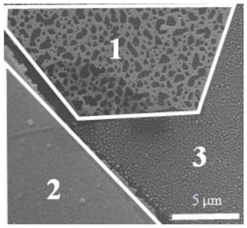
[0035] Using the same method as in Example 1, transfer ReS on heavily doped silicon or silicon dioxide substrates 2 thin slices, and deposited titanium / gold as contact electrodes on both sides of the material by electron beam lithography, and carried out the deposition of nano-gold layer and high-temperature annealing process. The scanning electron microscope image of the prepared sample is shown in image 3 shown. Among them: 1 is ReS 2 Gold on the sheet and surface; 2 is the electrode after annealing treatment; the figure shows the same as MoS 2 samples similar to the ReS 2 A gold nanolayer is formed on the surface of the flake.

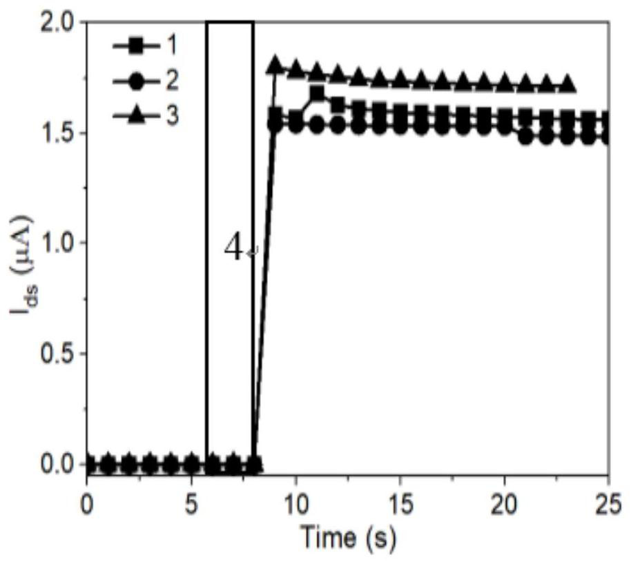
[0036] Figure 4 yes yes yes prepared ReS 2 Samples undergo real-time electrical and UV light response test graphs, such as Figure 4 As shown, the ultraviolet light occurs in the area shown in Figure 2, and the current remains at the microampere level after the ultraviolet light is removed. Position 1 in the figure is the time-varying chara...

Embodiment 3

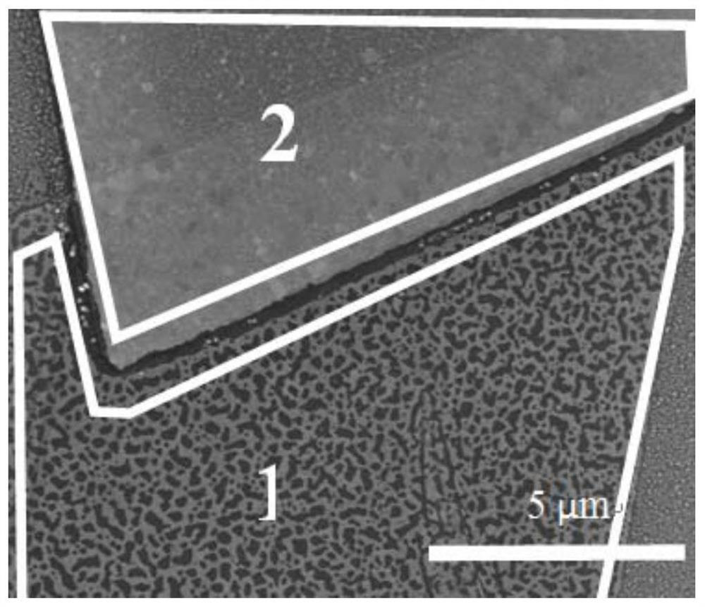
[0038] Using the same method as in Example 1, transfer MoSe on heavily doped silicon or silicon dioxide substrates 2 Thin slices, MoSe2 thin slices, followed by electron beam lithography to deposit titanium / gold on both sides of the material as contact electrodes, and perform nano-gold layer deposition and high-temperature annealing process. For the prepared MoS 2The sample is tested for long-term storage performance of optical signals. The first test time is 1000s. After the test, the sample is placed in a dark room environment, and the test is carried out after three days and seven days respectively. Keep at the microampere level. Curve 1 in the figure is the graph of the sample current changing with time in the air; Curve 2 is the test result after the sample was placed for three days; Curve 3 is the test result after the sample was placed for seven days.


PUM

PropertyMeasurementUnit
thicknessaaaaaaaaaa
thicknessaaaaaaaaaa

Abstract

The invention discloses an application of a photoelectric detection material in ultraviolet light detection. The photoelectric detection material is prepared according to the following method: step 1, transfer a transition metal chalcogenide sheet with a nanometer thickness to a substrate; step 2, in step 1. Depositing a gold nano-layer on the obtained device; step 3, annealing the device obtained in step 2, starting from a room temperature of 20°C-25°C at a rate of 5-15°C / min to 300°C-400°C, and keeping the temperature After 20 to 40 minutes, cool naturally to room temperature to obtain a photoelectric detection material; after the photoelectric detection material is irradiated with ultraviolet light, its current rises from the nanoampere level in the ground state to the microampere level, and can be turned off at the microampere level after the ultraviolet light is turned off. The electric current value is maintained for 15-20 days, and then placed in deionized water for cleaning and drying, and its electrical properties return to the ground state, and the photoelectric detection material can repeat this process cyclically. The invention has the advantages of high sensitivity and short response time.

Description

technical field [0001] The invention relates to the technical field of photoelectric sensing, in particular to the application of a photoelectric detection material in ultraviolet light detection. Background technique [0002] The detection of ultraviolet light is an important military and civilian technology. It has a wide range of applications in space communication, photoelectric countermeasures, missile plume monitoring, biomolecular and chemical molecule detection, ozone monitoring, organic pollution, and water quality inspection. At present, commercial ultraviolet detection devices are mainly silicon-based semiconductors and photomultiplier tubes. Silicon-based semiconductor devices still have a great response to the visible light region because of their forbidden band width of 1.2eV. In order to realize ultraviolet detection, it is necessary to add ultraviolet Filters increase the complexity of the device structure; the photomultiplier tube has the characteristics of ...

Claims


Application Information

Patent Timeline
Patent Type & Authority Patents(China)
IPC IPC(8): H01L31/18H01L31/032H01L31/113
CPCH01L31/18H01L31/1864H01L31/032H01L31/113Y02P70/50
Inventor 刘晶张荣杰
Owner TIANJIN UNIV
Why Eureka
Try Eureka