A kind of heterojunction, its preparation method and application

A heterojunction, antimony sulfide technology, applied in final product manufacturing, sustainable manufacturing/processing, climate sustainability, etc., can solve problems such as low photoelectric conversion efficiency of solar cells, improve transmission and collection efficiency, and facilitate the process. Feasible, reproducible results

Active Publication Date: 2021-02-26
HUAZHONG UNIV OF SCI & TECH +1
View PDF4 Cites 0 Cited by
  • Summary
  • Abstract
  • Description
  • Claims
  • Application Information

AI Technical Summary

Problems solved by technology

[0003] Aiming at the above defects or improvement needs of the prior art, the present invention provides a heterojunction comprising an antimony sulfide thin film epitaxially grown in [hk1] orientation, its preparation method and application, including a substrate and its surface with [hk1] The antimony sulfide thin film grown epitaxially, the substrate and the antimony sulfide thin film form a heterojunction structure, the epitaxially grown antimony sulfide thin film serves as the light absorbing layer of the solar cell, and the substrate film serves as the electron transport layer of the solar cell, thus solving the problem of The technical problem of low photoelectric conversion efficiency of existing solar cells using antimony sulfide thin films as light absorbing layers

Method used


Image

  • A kind of heterojunction, its preparation method and application
  • A kind of heterojunction, its preparation method and application
  • A kind of heterojunction, its preparation method and application

Examples


preparation example Construction

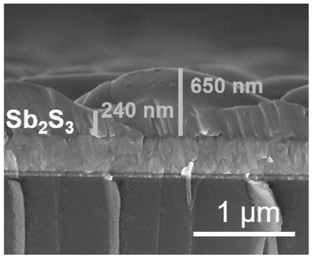
[0051] The present invention also provides the preparation method of the heterojunction, which exposes the substrate material to a crystal plane that matches the [hk1] orientation crystal plane of antimony sulfide, wherein h and k are integers, and 1 is the number 1 . At the same time, the substrate material also exposes atomic vacancies, which are oxygen vacancies or sulfur vacancies; the exposed oxygen vacancies or sulfur vacancies of the substrate material assist in inducing the epitaxial growth of antimony sulfide on the substrate surface.

[0052] In some embodiments, the substrate is annealed to cause a crystal phase transition to expose a crystal plane matching the [hk1] orientation crystal plane of the antimony sulfide, thereby inducing the epitaxial growth of the antimony sulfide on the substrate surface.

[0053] In some embodiments, the substrate is subjected to high-temperature annealing treatment to cause a crystal phase transition, from the traditional disordered...

Embodiment 1

[0074] A method for preparing a heterojunction comprising an antimony sulfide film epitaxially grown in [hk1] orientation, comprising the following steps:

[0075] (1) Substrate TiO 2 Preparation of: diisopropyl di(acetylacetonate) titanate (C 16 h 28 o 6 Ti) was mixed with absolute ethanol at a volume ratio of 1:9, and stirred for 24 hours to serve as a precursor solution. Wash the glass or conductive glass and spray the precursor solution at 450°C, where nitrogen is used as the carrier gas during the spraying process, and then kept at this temperature for 30 minutes and then cooled;

[0076] (2) Substrate TiO 2 Post-processing: the TiO described in step (1) 2 The sample is placed on a hot stage and annealed in air for 30-60 minutes at a temperature of 500°C.

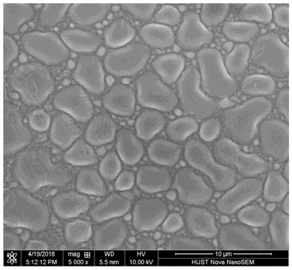
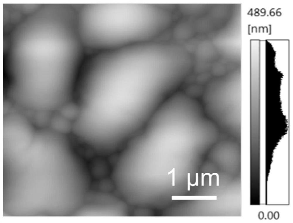
[0077] (3) Preparation of antimony sulfide film: Weigh 0.42g of antimony sulfide powder, sieve it three times with a 50-mesh sieve, so that the antimony sulfide powder can be evenly dispersed, and then sprinkle t...

Embodiment 2

[0083] A method for preparing a heterojunction comprising an antimony sulfide film epitaxially grown in [hk1] orientation, comprising the following steps:

[0084] (1) Substrate TiO 2 Preparation of: diisopropyl di(acetylacetonate) titanate (C 16 h 28 o 6Ti) was mixed with absolute ethanol at a volume ratio of 1:9, and stirred for 24 hours to serve as a precursor solution. Wash the glass or conductive glass and spray the precursor solution at 450°C, where nitrogen is used as the carrier gas during the spraying process, and then kept at this temperature for 30 minutes and then cooled;

[0085] (2) Substrate TiO 2 Post-processing: the TiO described in step (1) 2 The sample is placed on a hot stage and annealed in air for 30-60 minutes at a temperature of 500°C.

[0086] (3) Preparation of antimony sulfide film: Weigh 0.42g of antimony sulfide powder, sieve it three times with a 50-mesh sieve, so that the antimony sulfide powder can be evenly dispersed, and then sprinkle th...


PUM

PropertyMeasurementUnit
sizeaaaaaaaaaa
surface roughnessaaaaaaaaaa
band gapaaaaaaaaaa

Abstract

The invention belongs to the technical field of semiconductor thin film materials and solar cells, and particularly relates to a heterojunction, and a preparation method and an application thereof, inparticular to a heterojunction comprising an antimony sulfide thin film epitaxially grown in an orientation of [hK1], and a preparation method and an application of the heterojunction. The heterojunction comprises a substrate and the antimony sulfide thin film epitaxially grown on the surface of the substrate, wherein the substrate and the antimony sulfide thin film form a heterojunction structure; the antimony sulfide thin film is matched with the crystal surface of a substrate material; the antimony sulfide thin film is grown on the surface of the substrate in a molecular chain inclinationmanner; the growth orientation of the antimony sulfide thin film is mainly based on [hK1], wherein h and k are integers; and the surface of the antimony sulfide thin film has a light trapping effect.The antimony sulfide thin film epitaxially grown in the orientation of [hK1] is used as a light absorption layer of a solar cell, and a substrate thin film serves as an electron transport layer of thesolar cell, so that the technical problem that the photoelectric conversion efficiency of the solar cell taking the antimony sulfide thin film as the light absorption layer is low is solved.

Description

technical field [0001] The invention belongs to the technical field of semiconductor thin film materials and solar cells, and in particular relates to a heterojunction, its preparation method and application, especially to a heterojunction comprising an antimony sulfide thin film epitaxially grown in [hk1] orientation, and its Preparation methods and applications. Background technique [0002] Antimony sulfide is a low-cost, green, low-toxic, single-phase and stable binary compound with a band gap of 1.73eV and an absorption coefficient of 10 5 cm -1 . Antimony sulfide thin film is a kind of photoelectric material with excellent performance, which is suitable to be used as the absorber layer of battery, and this thin film has attracted extensive attention in the research field. At the same time, in the stacked battery structure, the band gap of the antimony sulfide thin film perfectly matches that of the crystalline silicon battery, but the performance of the antimony sul...

Claims


Application Information

Patent Timeline
Patent Type & Authority Patents(China)
IPC IPC(8): H01L31/0236H01L31/032H01L31/036H01L31/072H01L31/18
CPCH01L31/02363H01L31/032H01L31/036H01L31/072H01L31/18Y02E10/50Y02P70/50
Inventor 宋海胜侯腾轩邓辉张欢
Owner HUAZHONG UNIV OF SCI & TECH
Why Eureka
Try Eureka