Integrated low-capacitance ESD protection device and preparation method thereof

An ESD protection, low-capacitance technology, applied in the fields of electrical solid-state devices, semiconductor/solid-state device manufacturing, electrical components, etc., can solve the problems of reduced ESD leakage capability, increased chip area, and low discharge current value, to ensure ESD leakage capability, uniform current distribution, and small transient on-state voltage drop

Pending Publication Date: 2019-09-20
江苏吉莱微电子股份有限公司 +1
View PDF0 Cites 1 Cited by
  • Summary
  • Abstract
  • Description
  • Claims
  • Application Information

AI Technical Summary

Problems solved by technology

[0003] From the design structure of ESD protection devices, there are mainly diode structure, triode structure, thyristor structure, etc. The diode structure mainly uses the clamp protection function of diode reverse breakdown voltage to discharge ESD. Its advantages are simple process and low cost. The disadvantage is that the reverse breakdown voltage of the diode increases gradually with the increase of the discharge current, so that the value of the discharge current it bears is low. In addition, the breakdown of the diode is an avalanche breakdown, and the concentration on both sides of the PN junction is high. Therefore, the capacitance value is relatively large, usually above 100pF
The triode structure mainly uses the voltage BVCEO between the collector and emitter of the triode to discharge the ESD current. Its advantage is that the BVCEO value is low. Compared with the diode structure, it can discharge higher ESD current. The disadvantage is that its The capacitance value is still large, usually above 5pF
The disadvantage is that, due to the introduction of series resistors such as copper wires in this connection method, the overall ESD leakage capability is significantly reduced, so the area of ​​the chip needs to be increased and the cost is increased.

Method used


Image

  • Integrated low-capacitance ESD protection device and preparation method thereof
  • Integrated low-capacitance ESD protection device and preparation method thereof
  • Integrated low-capacitance ESD protection device and preparation method thereof

Examples


Embodiment Construction

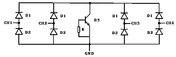
[0036] Such as figure 1 It is an equivalent circuit diagram of the present invention, an integrated low-capacitance ESD protection device, which is a four-channel low-capacitance unidirectional integrated ESD protection device, and the direction of ESD leakage is: CH1 to GND, and the channel flows through the low-capacitance diode D1 and the low-voltage The diode D3 is connected to the ground, and the low-voltage diode D3 is the main part of the ESD discharge. D3 is a triode structure in which EB is short-circuited. The IV characteristic between C and E is used to realize the discharge of the ESD current. The residual voltage of the structure is lower than that of the conventional diode structure using reverse avalanche breakdown voltage leakage, and there is no latch-up effect of the thyristor structure. From GND to CH1, the current flows through the low-capacity diode D2 to CH1, and the low-capacity diode D2 is forward-conducting. Since the capacitance of the diode D3 is mu...


PUM


Abstract

The invention discloses an integrated low-capacitance ESD protection device and a preparation method thereof. The integrated device comprises low-capacitance one-way integrated ESD protection devices of four channels; each channel is composed of a low-capacitance diode D1 and a low-capacitance diode D2 which are connected in series; and the four channels are connected with a low-voltage diode D3 in parallel. The preparation method of the integrated low-capacitance ESD protection device comprises the following steps: preparing a P+ substrate material; carrying out photoetching and arsenic injection and annealing; carrying out epitaxial growth; carrying out photoetching and boron injection and annealing; carrying out photoetching and STI isolation preparation; carrying out photoetching and boron injection and annealing; carrying out photoetching and phosphorus injection and annealing; photoetching contact holes; sputtering metal on the front surface; carrying out photoetching to form a front metal area 10; thinning the back surface; carrying out silver or gold evaporation on the back surface; and forming vacuum alloy. Three chips and the diodes D1, D2 and D3 are integrated on a chip, and the performance requirements of high ESD discharge current, low capacitance and low residual voltage are met at the same time.

Description

technical field [0001] The invention relates to the technical field of semiconductor devices and semiconductor technology, in particular to an integrated low-capacitance ESD protection device and a preparation method thereof. Background technique [0002] As the process size of semiconductor devices continues to shrink, the application environment of circuits becomes more and more complex, and the frequency and impact of Electrostatic Discharge (ESD, Electrostatic Discharge) that integrated circuits face will increase accordingly. On the interface side of consumer electronics applications, such as DVI (Digital Visual Interface, Digital Visual Interface), VGA (Video Graphics Array Interface, Video Graphics Array Interface) USB (Universal Serial Bus, Universal Serial Bus), HDMI (High Definition Digital Interface , High Definition Multimedia Interface) etc. are often impacted by ESD. With the continuous improvement of data transmission speed requirements, the impact current du...

Claims


Application Information

Patent Timeline
Patent Type & Authority Applications(China)
IPC IPC(8): H01L27/02H01L21/822
CPCH01L21/822H01L27/0255H01L27/0296
Inventor 宋文龙
Owner 江苏吉莱微电子股份有限公司
Why Eureka
Try Eureka