Pixel unit of perovskite image sensor and preparation method thereof

A pixel unit and perovskite technology, applied in the field of perovskite infrared pixel unit devices and their preparation, can solve the problems of poor performance of metal oxide thin film transistors, increase in absolute value of threshold voltage, and increase in sub-threshold swing. , to achieve the effect of fast production speed, good uniformity and strong absorption characteristics

Active Publication Date: 2019-09-24
PEKING UNIV SHENZHEN GRADUATE SCHOOL
View PDF3 Cites 8 Cited by
  • Summary
  • Abstract
  • Description
  • Claims
  • Application Information

AI Technical Summary

Problems solved by technology

[0003] In the process of realizing the present invention, the inventors have found that there are at least the following problems in the prior art: the performance of organic-inorganic hybrid infrared detection perovskite photodiodes becomes poor after patterning; The deterioration of transistor performance is specifically manifested in the increase of dark current, the increase of sub-threshold swing, and the increase of the absolute value of threshold voltage.

Method used


Image

  • Pixel unit of perovskite image sensor and preparation method thereof
  • Pixel unit of perovskite image sensor and preparation method thereof
  • Pixel unit of perovskite image sensor and preparation method thereof

Examples


preparation example Construction

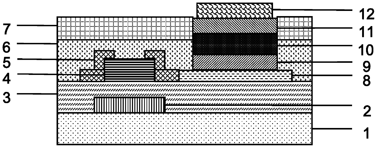
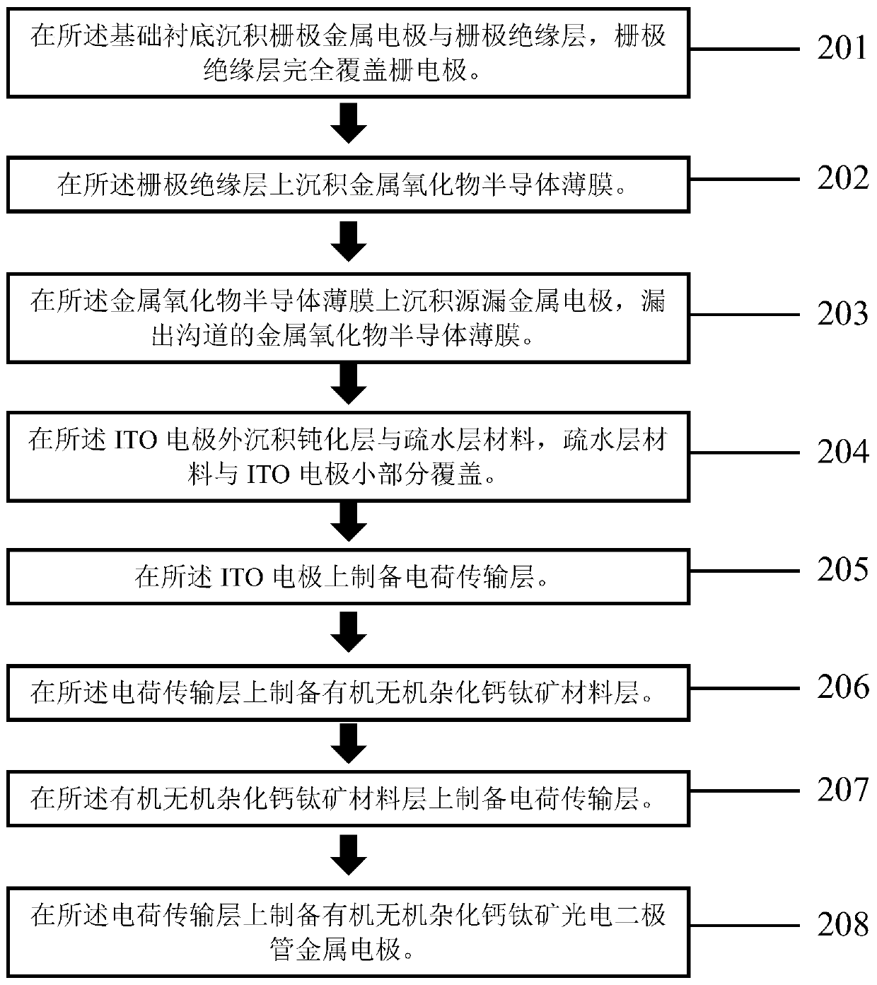
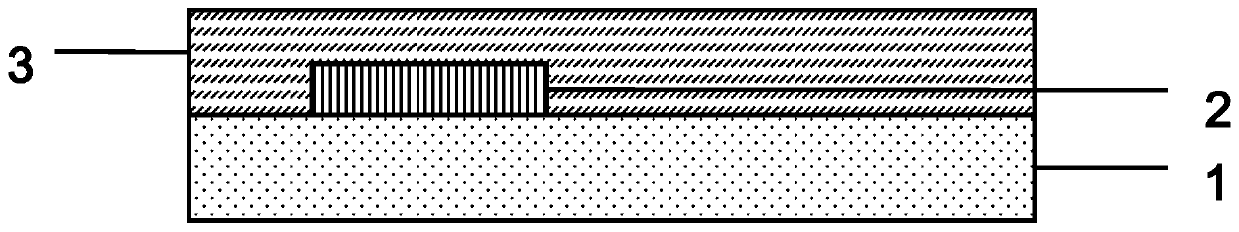
[0062] Such as image 3 As shown, it is a flowchart of a method for preparing a perovskite infrared pixel unit according to an embodiment of the present invention, and the method includes:

[0063] 201. Deposit the gate metal electrode 2 and the gate insulating layer 3 on the base substrate, and the gate insulating layer 3 completely covers the gate electrode 2; please refer to image 3 , image 3 It is a schematic diagram of the structure after depositing the gate metal electrode 2 and the gate insulating layer 3 in Embodiment 1 of the present invention, and the source-drain metal electrode 4 is in the shape of a block or interdigitated.

[0064] 202. Deposit a metal oxide semiconductor thin film 4 on the source gate insulating layer 3; please also refer to Figure 4 , Figure 4 It is a schematic structural diagram after depositing a metal oxide semiconductor thin film in Example 1 of the present invention.

[0065] 203. Deposit source-drain metal electrodes 5 on the meta...


PUM

PropertyMeasurementUnit
thicknessaaaaaaaaaa
thicknessaaaaaaaaaa
thicknessaaaaaaaaaa

Abstract

The embodiment of the invention provides a pixel unit of an image sensor based on perovskite photosensitive material and a preparation method thereof. A photosensitive pixel unit comprises a metal oxide thin film transistor and an organic-inorganic hybrid perovskite photodiode. The metal oxide thin film transistor comprises a base substrate, a gate metal electrode, a gate insulating lay, a metal oxide semiconductor thin film, a source / drain metal electrode, a silicon dioxide protection layer and a hydrophobic layer thin film. The organic-inorganic hybrid perovskite photodiode comprises an indium tin oxide ITO electrode, a pattern electron transport layer, an organic-inorganic hybrid perovskite material layer, a charge transport layer and a metal electrode.

Description

technical field [0001] The invention relates to the field of photodetectors, in particular to a perovskite infrared pixel unit device and a preparation method thereof. Background technique [0002] Metal oxide semiconductor thin film transistors, especially indium gallium zinc oxide (IGZO) thin film transistors have the characteristics of stability, high mobility, transparency, and good uniformity, and are widely used in display panel arrays and detector arrays, but IGZO materials are due to Its forbidden band width is relatively large (>3eV), and it has no obvious response to the visible light band above 420nm. Organic-inorganic hybrid perovskite materials have the characteristics of wide light absorption range, high carrier mobility, fast carrier generation speed, long carrier diffusion length, and long carrier lifetime. Organic-inorganic hybrid calcium The excellent light absorption characteristics of titanium ore materials make it widely used in the field of photodet...

Claims


Application Information

Patent Timeline
Patent Type & Authority Applications(China)
IPC IPC(8): H01L27/146
CPCH01L27/146H01L27/14605H01L27/1462H01L27/14683
Inventor 周航王娅
Owner PEKING UNIV SHENZHEN GRADUATE SCHOOL
Why Eureka
Try Eureka