In-chip embedded diamond heat dissipation gallium nitride transistor based on etching and directional epitaxy and preparation method thereof
A gallium nitride and transistor technology, which is applied in the field of thermal management development of power semiconductor devices, can solve the problems of increasing the heat accumulation effect in the active area of the chip, poor thermal conductivity, and degradation of device performance and reliability, so as to improve high-efficiency heat dissipation characteristics, The effect of efficient heat dissipation
- Summary
- Abstract
- Description
- Claims
- Application Information
AI Technical Summary
Problems solved by technology
Method used
Image
Examples
preparation example Construction
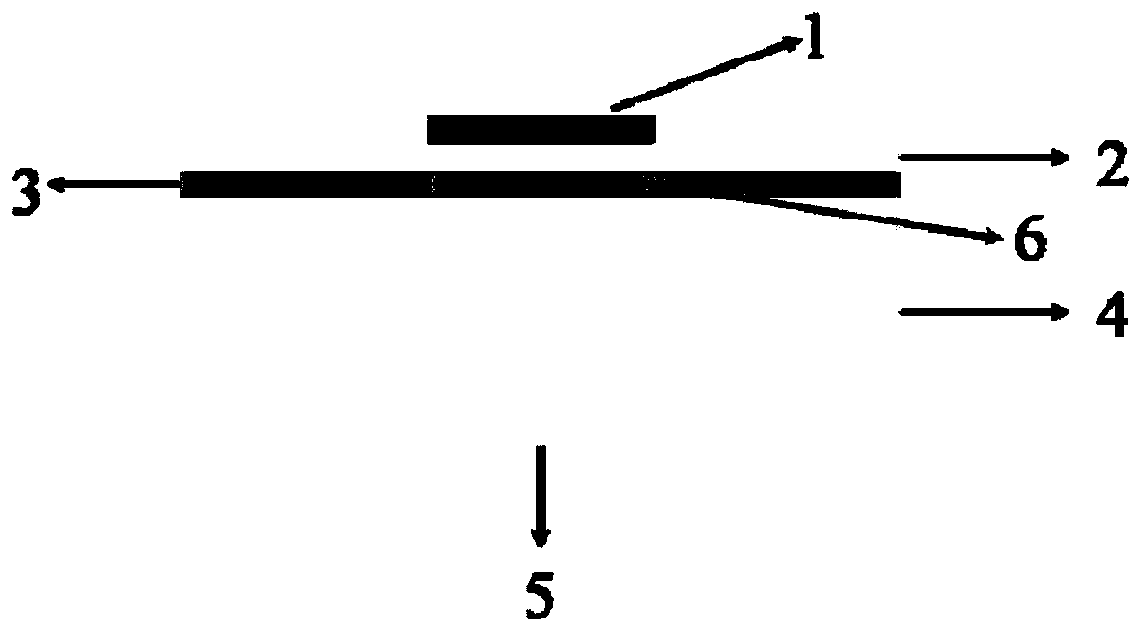
[0018] Referring to Fig. 2, the fabrication method of the on-chip embedded diamond heat-dissipating gallium nitride transistor based on etching and directional epitaxy includes the following specific steps:
[0019] 1) Preparation of on-chip embedded diamond heat sink based on etching and directional epitaxy;
[0020] ①Barrier layer protection of SiC substrate: grow the protective layer on the barrier layer of SiC substrate, the growth method is sputtering or evaporation, the protective layer is made of SiN material, the thickness of the protective layer is 100-200nm, and the temperature is controlled below 350°C , as shown in Figure 2(a);
[0021] ② SiC substrate backside thinning and polishing: use the combination of temporary bonding and polishing process to carry out backside thinning of SiC substrate. The thickness of the thinned substrate is controlled at 150-200 microns, and then the bonding carrier is removed. The bonding carrier is made of sapphire or silicon carbide...
Embodiment
[0030] A method for designing and manufacturing a gallium nitride transistor embedded in a diamond heat sink in a near-junction region, specifically comprising:
[0031] 1) Fabrication of an in-chip diamond-embedded high-efficiency heat dissipation zone based on etching and directional epitaxy;
[0032] ①Grow the protective layer on the barrier layer of the SiC substrate, sputter the protective layer of SiN material with a thickness of 100nm, and control the growth temperature at 300°C;
[0033] ②Using sapphire as a bonding carrier, spin-coat high-temperature wax on the sapphire and perform temporary bonding with the front of the wafer, thin and polish the back of the SiC substrate to 200um, and then remove the bonding carrier;
[0034] ③The Ti / Au layer is sputtered after the mask pattern is realized on the back of the SiC substrate by photolithography, and the substrate is peeled off and engraved. The area cross section size is 250*200um;
[0035] ④Use a plasma etching mach...
PUM
| Property | Measurement | Unit |
|---|---|---|
| thickness | aaaaa | aaaaa |
Abstract
Description
Claims
Application Information


