Preparation method, product, and applications of cetyl trimethyl ammonium bromide modified bismuth molybdate photoelectrode
A technology of hexadecyltrimethylammonium bromide and bismuth molybdate, which is applied in chemical instruments and methods, light water/sewage treatment, water pollutants, etc., can solve the problems of limited popularization and application, high recombination rate of photogenerated charges, and Problems such as unsatisfactory photocatalytic activity
- Summary
- Abstract
- Description
- Claims
- Application Information
AI Technical Summary
Problems solved by technology
Method used
Image
Examples
Embodiment 1
[0033] Step 1: Preparation of bismuth molybdate powder by hydrothermal method
[0034] Take 1mol / L Na 2 MoO 4 2H 2 O solution 50ml and 2mol / L Bi(NO 3 ) 3 ·5H 250ml of O solution was thoroughly mixed to obtain a bismuth molybdate precursor solution, adjusted to a pH value of 9 with NaOH, placed in a hydrothermal reaction kettle, and subjected to a hydrothermal reaction at 120°C for 24 hours, and filtered after the hydrothermal reaction was completed. Dry and grind at 60°C to obtain bismuth molybdate powder;
[0035] Step 2: Preparation of bismuth molybdate photoelectrode
[0036] Add 0.15g of bismuth molybdate powder prepared in step 1 to 10ml of water to make a bismuth molybdate suspension, add 2mL of polyethylene glycol 400 and stir evenly, then add 0.1g of ethanol, heat and stir at 70°C until completely dissolved, and obtain a viscous Suspension, the suspension is evenly scraped onto the FTO conductive glass, the thickness of the film layer is 45 μm, placed in an oven...
Embodiment 2
[0038] The preparation process is the same as in Example 1, the difference is that 0.04mol of CTAB is added to the uniformly mixed bismuth molybdate precursor solution in step 1 to obtain a CTAB-modified bismuth molybdate photoelectrode (BMO-1);
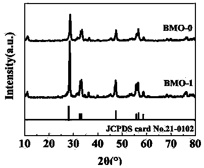
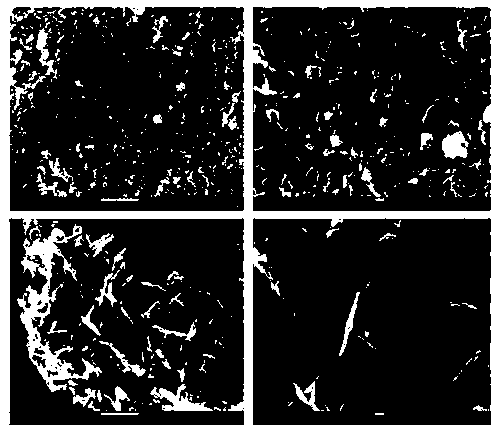
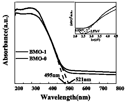
[0039] The photoelectrode prepared in embodiment 1 and embodiment 2 is carried out structure and morphology analysis, and the X-ray diffraction spectrum (XRD) of implementing 1 photoelectrode and embodiment 2 photoelectrode is as follows figure 1 As shown, several groups of enhanced diffraction peaks 2θ=28.24°, 32.59°, 33.07°46.72°, 55.45°, 56.16° and 58.42° can be observed in the spectrum, corresponding to (131), (002), (060) , (202), (331), (262) crystal planes, the positions of the diffraction peaks and Bi 2 MoO 6 The XRD standard card (JCPDS 21-0102) matches, all belong to the orthorhombic crystal phase, and no other impurity phases appear, indicating that the purity is high. After calcining in the muffle furnace, it can be see...
PUM
 Abstract
Description
Claims
Application Information


