A high-speed low-power high-voltage power device

A high-voltage power device, low power consumption technology, applied in the direction of semiconductor devices, electrical components, circuits, etc., can solve the problems that affect the uniformity and reliability of device current distribution, reduce the efficiency of anode hole injection, and limit the parallel use of devices. Achieve the effects of eliminating voltage foldback, low conduction voltage drop, and fast turn-off speed

Active Publication Date: 2020-09-29
UNIV OF ELECTRONICS SCI & TECH OF CHINA +1
View PDF4 Cites 0 Cited by
  • Summary
  • Abstract
  • Description
  • Claims
  • Application Information

AI Technical Summary

Problems solved by technology

However, the introduction of the traditional short-circuited anode structure, on the one hand, makes the device switch from the unipolar conduction mode to the bipolar conduction mode during the turn-on process, resulting in a voltage foldback effect, which affects the uniformity and reliability of the current distribution of the device, and limits the performance of the device. On the other hand, the short-circuited anode structure will reduce the injection efficiency of the anode holes and increase the conduction voltage drop

Method used


Image

  • A high-speed low-power high-voltage power device
  • A high-speed low-power high-voltage power device
  • A high-speed low-power high-voltage power device

Examples


Embodiment 1

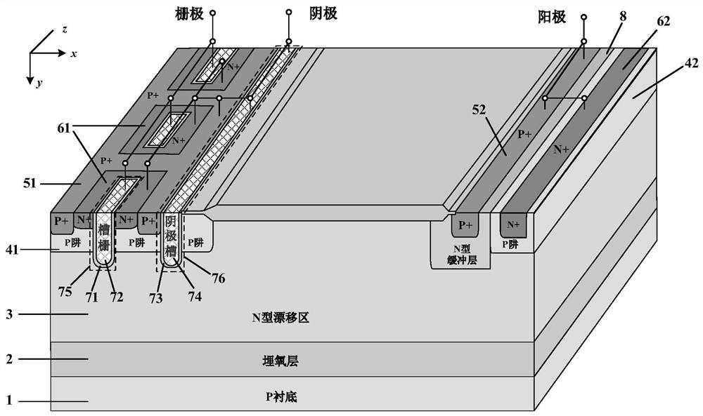
[0016] Such as figure 1 As shown, the SOI LIGBT structure of this example includes a P substrate 1, a buried oxide layer 2, and an N-type drift region 3 stacked sequentially from bottom to top; one side of the surface of the N-type drift region 3 is a cathode structure and a groove structure, the other side is the anode structure;

[0017] The cathode structure includes a P well region 41, a P+ cathode region 51 and an N+ cathode region 61, wherein the P+ cathode region 51 and the N+ cathode region 61 are located on the top of the P well region 41, and the P+ cathode region 51 and the N+ cathode region 61 The common lead-out end of is a cathode; The groove structure includes a segmented groove grid 75 and a cathode groove 76, wherein the cathode groove 76 is closer to the anode structure; the groove bottom and side walls of the segmented groove grid 75 cover the first insulating The dielectric layer 71, the first insulating dielectric layer 71 surrounds the first conductive m...

Embodiment 2

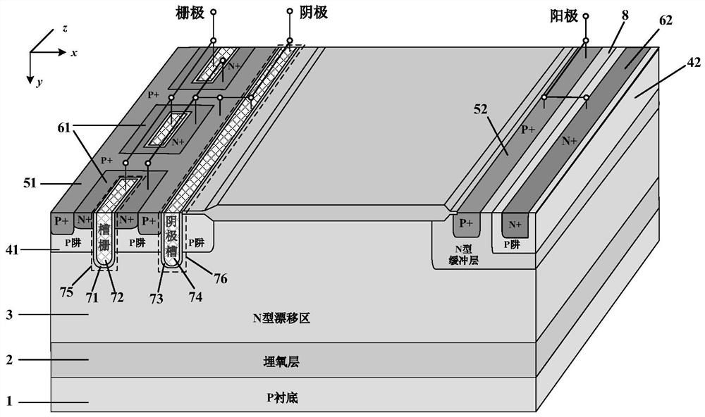
[0022] Such as figure 2 As shown, compared with Embodiment 1, the P well region 42 in this example is located on the upper part of the N-type buffer layer 8, which is beneficial to improve the withstand voltage characteristics of the device, and further increase the turn-off speed of the device to reduce the turn-off speed. loss.

Embodiment 3

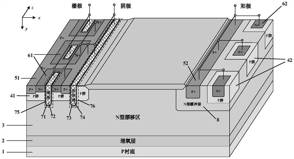
[0024] Such as image 3 As shown, compared with Embodiment 2, the anode terminal in this example is distributed in sections in the longitudinal direction by the P well region 42 and the N+ anode region 62, and the upper part of each section of the P well region 42 has the N+ anode Region 62, this segmented distribution method can increase the area of ​​the parasitic NPN tube composed of N+ anode region 62 / P well region 42 / N-type buffer layer 8, which increases the electron extraction path during the device shutdown process, which is conducive to further Accelerates device turn-off and reduces turn-off losses.


PUM


Abstract

The invention belongs to the technical field of power semiconductors and in particular relates to a high voltage power device with high speed and low power consumption. Compared with the traditional short circuit anode, a new structure places an N+ anode region in a P well region, and a cathode terminal adopts a segmented groove gate and a cathode groove structure. During forward conduction, a P well region of an anode terminal is taken as a potential barrier of an electron and can eliminate voltage return effect, the segmented groove gate increases channel density of the device, so as to reduce resistance of a channel region of the device, and the cathode groove physically blocks a hole from being quickly pumped out by a P+ cathode region, so as to improve conductivity modulation effect,thus lower conduction voltage drop is obtained; in a process of turning off the device, the anode terminal is enabled by virtue of a parasitic thin base region NPN transistor formed by an N+ anode region / a P well region / a N type buffer layer, pumping-out of electrons stored in a drift region is accelerated, turn-off speed of the device is increased, and turn-off loss is reduced. Compared with thetraditional short circuit anode structure, the high voltage power device provided by the invention eliminates the voltage return phenomenon in a smaller cellular size and has lower conduction voltagedrop and turn-off loss.

Description

technical field [0001] The invention belongs to the technical field of power semiconductors, and relates to a slot-gate short-circuited anode SOI LIGBT (Lateral Insulated Gate Bipolar Transistor, lateral insulated gate bipolar transistor). Background technique [0002] IGBT is a new device combining MOSFET (Metal Oxide Semiconductor Field Effect Transistor) and BJT (Bipolar Junction Transistor). It not only has the advantages of high input impedance of MOSFET and low on-resistance of BJT, but also realizes High breakdown voltage and high forward current. Among them, lateral IGBT (LIGBT) is easy to be integrated in silicon-based, especially SOI-based power integrated circuits. SOI-based LIGBT can completely eliminate the hole-electron injection of bulk silicon LIGBT substrate, and the use of dielectric isolation SOI technology is easy to achieve device integration. Complete electrical isolation makes SOI LIGBT widely used in high-tech industries such as power electronics, in...

Claims


Application Information

Patent Timeline
Patent Type & Authority Patents(China)
IPC IPC(8): H01L29/739H01L29/423
CPCH01L29/42304H01L29/7397
Inventor 罗小蓉王晨霞鲁娟郗路凡马臻黄俊岳宋旭魏杰杨永辉朱坤峰
Owner UNIV OF ELECTRONICS SCI & TECH OF CHINA
Why Eureka
Try Eureka