High-speed DFB laser and manufacturing method thereof

A DFB laser, high-speed technology, applied in the direction of lasers, laser components, semiconductor lasers, etc., can solve the problems of DFB laser bandwidth limitation, reduce device heat dissipation characteristics, reduce chip heat dissipation area, etc., to achieve good lattice matching and modulation rate Fast, quality-enhancing results

Pending Publication Date: 2019-12-03
全磊光电股份有限公司
View PDF5 Cites 6 Cited by
  • Summary
  • Abstract
  • Description
  • Claims
  • Application Information

AI Technical Summary

Problems solved by technology

These methods can obtain high-speed modulated DFB lasers, but some of these processes reduce the heat dissipation characteristics of the device while increasing the modulation bandwidth of the laser, for example: reducing the cavity length, that is, reducing the heat dissipation area of ​​the chip; using polymers instead of semiconductors as electrodes The support layer reduces the heat dissipation coefficient of the material, etc. These factors lead to the limitation of the bandwidth of the DFB laser when it works at high temperature
[0005] To this end, Macom uses a chip with a size of 200*250um, but in the ridge area of ​​the chip, part of the active area is etched away, and the cavity length of the chip is shortened without changing the heat dissipation area of ​​the chip to obtain a high-bandwidth DFB laser; In addition, Oclaro uses the InGaAsP waveguide layer to replace part of the active region to reduce the confinement factor and increase the bandwidth; however, because the quantum well material is a material containing Al, it is easy to oxidize and form defects during the etching and growth process, which easily leads to high-speed Lasers fail under high temperature operating conditions

Method used


Image

  • High-speed DFB laser and manufacturing method thereof
  • High-speed DFB laser and manufacturing method thereof
  • High-speed DFB laser and manufacturing method thereof

Examples


preparation example Construction

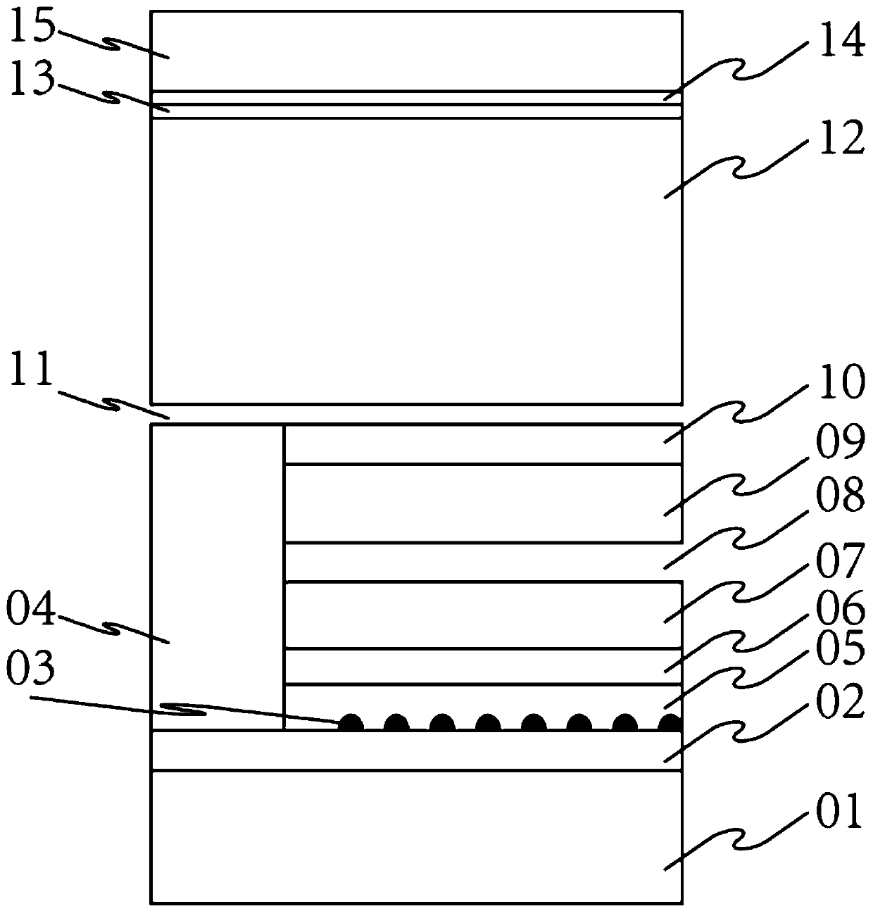
[0030] A preparation method for a high-speed DFB laser, comprising the steps of:

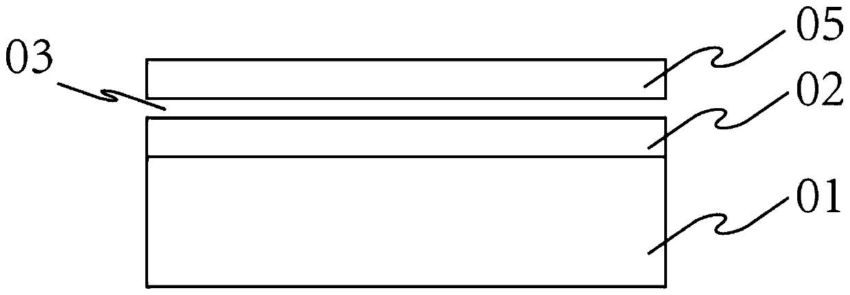
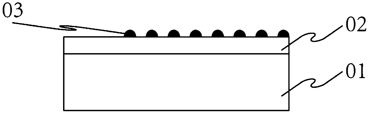
[0031] Step 1: Using InP as the growth substrate, the buffer layer 02 and the grating layer are sequentially grown on the InP substrate 01 to obtain the first epitaxial structure, such as figure 2Then take out the epitaxial wafer, spin-coat photoresist, use holographic lithography or electron beam lithography to form a grating pattern, and then use optical lithography to define the first waveguide region, and use chemical wet etching method to form a partial raster; as in image 3 shown.

[0032] Step 2: Carry out the second epitaxial growth on the basis of step 1; first, in the pH 3 Under the protection of gas, slowly raise the temperature to 550°C, and then feed TMIn in pulses as the source gas to grow InP. When the thickness of the InP layer 050 completely covers the grating, raise the temperature to the normal epitaxial growth temperature of 670°C, increase the flow rate of TMIn, from Ra...

specific Embodiment

[0040] With a conductivity of 2-8x10 18 cm -2 The InP is used as the growth substrate and put into the MOCVD system of Aixtron Company for growth. The reaction chamber pressure was 50mbar, the growth temperature was 670°C, and the 2 As carrier gas, trimethylindium (TMIn), trimethylgallium (TMGa), trimethylaluminum (TMAl), diethylzinc (DeZn), silane (SiH 4 ), arsine (AsH 3 ) and phosphine (PH 3 ) and the like are reaction source gases, and sequentially grow an N-InP buffer layer, an N-InGaAsP grating layer, and an N-InP transition layer. Among them, the thickness of the grating layer is 50nm. It is worth noting that the grating layer N-InGaAsP is a tensile strain, and the strain is 500-1000ppm.

[0041] Then the grown epitaxial wafer is taken out, and a grating is formed by holographic lithography or electron beam lithography. The grating period is 203nm and the depth is 70nm. At the same time, the wave layer region B is formed by optical lithography, and the width of the...


PUM


Abstract

The invention provides a high-speed DFB laser, and the epitaxial structure thereof comprises an InP substrate. A buffer layer is deposited on the InP substrate. A vertical confinement layer is deposited on the upper left of the buffer layer. A grating layer, a transition layer, a lower confinement layer in an active area, a lower waveguide layer, a quantum well, an upper waveguide layer and an upper confinement layer in the active area are deposited on the upper right of the buffer layer in order from bottom to top. The vertical confinement layer is aligned with the upper end of the upper confinement layer in the active area, and a corrosion barrier layer is deposited above the two layers. A coupling layer, a first barrier gradation layer, a first barrier gradation layer and an ohmic contact layer are sequentially deposited on the corrosion barrier layer. According to the invention, the laser has the advantages of low resistance, fast modulation rate and good lattice matching at high temperature, and is favorable for grating preservation; and during the growth process, pulsed airflow growth is used to grow a microscler nucleus layer first and then an epitaxial layer with a certainthickness, which is beneficial to improve the growth quality of the epitaxial layer.

Description

technical field [0001] The invention belongs to the technical field of DFB laser development, and in particular relates to a high-speed DFB laser and a manufacturing method thereof. Background technique [0002] As the 5G commercialization is approaching, the dynamic single-mode distributed feedback laser (DFB-LD) with narrow linewidth, high side mode suppression ratio and high modulation rate has become the preferred light source. DFB adopts grating modulation with periodically changing refractive index, has good single longitudinal mode characteristics, side mode suppression ratio can reach more than 35dB, and modulation rate can reach more than 50GHz, which can meet the application requirements of high speed / low delay of 5G mobile network. Since the 5G network is used outdoors, it is required to achieve a high modulation rate at -40 to 85°C. However, at high temperatures, the carrier leakage of the laser is serious, and the excessive hot phonons are easy to kick the carri...

Claims


Application Information

Patent Timeline
Patent Type & Authority Applications(China)
IPC IPC(8): H01S5/12H01S5/22H01S5/34H01S5/343
CPCH01S5/1228H01S5/22H01S5/1231H01S5/34313H01S5/3403
Inventor 单智发张永姜伟陈阳华
Owner 全磊光电股份有限公司
Why Eureka
Try Eureka