Epitaxial growth method of BaSi2 film
An epitaxial growth and thin film technology, applied in the directions of crystal growth, single crystal growth, single crystal growth, etc., can solve the problems of high cost and low rate in molecular beam epitaxy growth, and achieve high quality, low cost and good epitaxial characteristics. Effect
- Summary
- Abstract
- Description
- Claims
- Application Information
AI Technical Summary
Problems solved by technology
Method used
Image

Examples
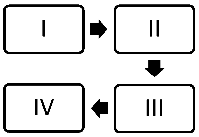
Embodiment 1
[0033] In step I, the substrate was ultrasonically cleaned in acetone, ethanol, and deionized water for 5 min each. Then put it in the acid solution of 80°C hydrochloric acid: hydrogen peroxide: water = 1:1:5 and the alkali solution of 80°C ammonia: hydrogen peroxide: water = 1:1:5 to wash for 5 minutes, and finally remove it in 5% dilute HF. The oxide layer was rinsed with deionized water and dried with high-purity nitrogen for later use.
[0034] The substrate cleaned in step II is introduced into the magnetron sputtering vacuum chamber, and the vacuum is drawn to 5×10 -5 Below Pa, raise the substrate temperature to 850°C and maintain it for 30min, then lower the substrate temperature to 500°C.
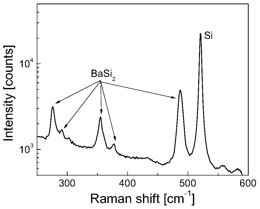
[0035] Step III sputters a Ba layer on a substrate at 500°C, the sputtering pressure is 0.3Pa, the sputtering rate is 2.5nm / min, and the sputtering time is 2min. During this process, Ba reacts with the heated Si substrate to form BaSi 2 Seed layer, detected by Raman spectroscopy,...
PUM
 Abstract
Description
Claims
Application Information
 - R&D
- Intellectual Property
- Life Sciences
- Materials
- Tech Scout
- Unparalleled Data Quality
- Higher Quality Content
- 60% Fewer Hallucinations
Browse by: Latest US Patents, China's latest patents, Technical Efficacy Thesaurus, Application Domain, Technology Topic, Popular Technical Reports.
© 2025 PatSnap. All rights reserved.Legal|Privacy policy|Modern Slavery Act Transparency Statement|Sitemap|About US| Contact US: help@patsnap.com