

Micro-nanoparticle reinforced high-indium copper-based active solder and preparation method thereof
A technology of micro-nano particles and active brazing filler metal, applied in manufacturing tools, welding equipment, metal processing equipment, etc., to reduce melting temperature, reduce residual stress of brazing, and optimize microstructure
- Summary
- Abstract
- Description
- Claims
- Application Information
AI Technical Summary
Problems solved by technology
Method used
Image


Examples
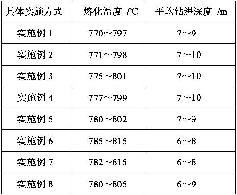
Embodiment 1
[0043] A high-indium copper-based active solder reinforced by micro-nano particles, the high-indium copper-based active solder reinforced by micro-nano particles includes the following raw materials in parts by weight: 85 parts of basic components, 10 parts of active components, trace amounts 0.2 parts of components and 4.8 parts of micro-nano reinforcing particles; wherein, the basic components include the following components by weight: 15 parts of indium, 4 parts of tin, 1 part of manganese, 2 parts of phosphorus, 0.5 parts of antimony, 0.5 parts of Silicon, 1 part of germanium and the balance of copper; the active component includes the following components in parts by weight: 85 parts of titanium and 15 parts of chromium; the trace component is rare earth cerium; the above components are respectively centered on copper indium Alloy, copper-tin master alloy, copper-manganese master alloy, copper-phosphorus master alloy, copper-antimony master alloy, copper-silicon master al...
Embodiment 2
[0065] The difference between this embodiment and Example 1 is that the raw materials are weighed according to the following parts by weight: 88 parts of basic components, 9 parts of active components, 0.3 parts of trace components and 2.7 parts of micro-nano reinforcing particles; the basic components The element includes 14 parts of indium, 4 parts of tin, 1 part of manganese, 3 parts of phosphorus, 0.8 part of antimony, 0.8 part of silicon, 2 parts of germanium and the balance copper by weight; the active component includes 80 parts of titanium and 20 parts of chromium, its preparation method is identical with embodiment 1.
Embodiment 3
[0067] The difference between this embodiment and Example 1 is that the raw materials are weighed according to the following parts by weight: 90 parts of basic components, 7 parts of active components, 0.5 parts of trace components and 2.5 parts of micro-nano reinforcing particles; the basic components The element includes 12 parts by weight of indium, 5 parts of tin, 1.5 parts of manganese, 3.5 parts of phosphorus, 1 part of antimony, 1 part of silicon, 2 parts of germanium and the balance of copper; the active component includes 75 parts of titanium and 25 parts of chromium, its preparation method is identical with embodiment 1.
PUM
| Property | Measurement | Unit |
|---|---|---|
| particle diameter | aaaaa | aaaaa |
| melting point | aaaaa | aaaaa |
Abstract
Description
Claims
Application Information