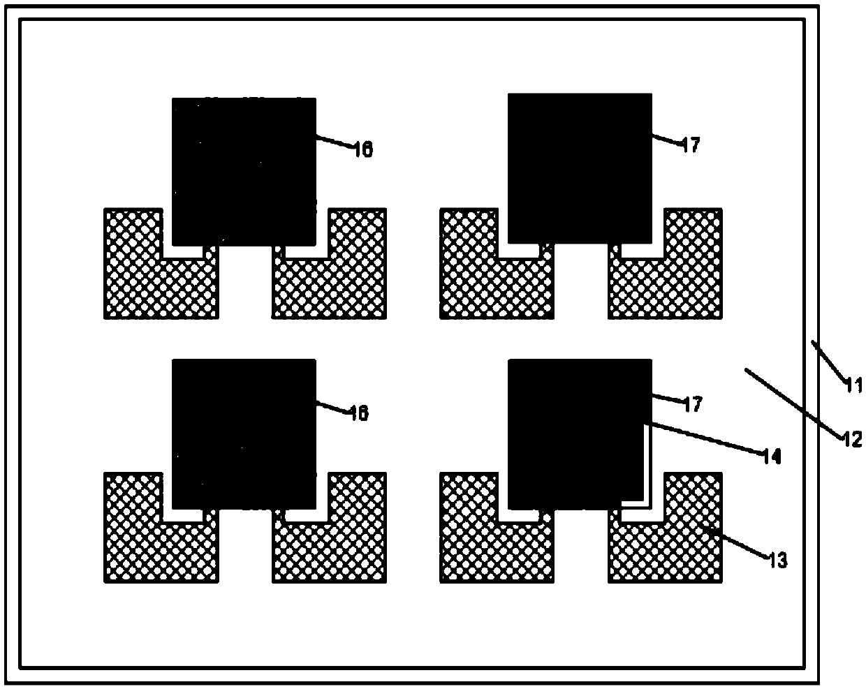
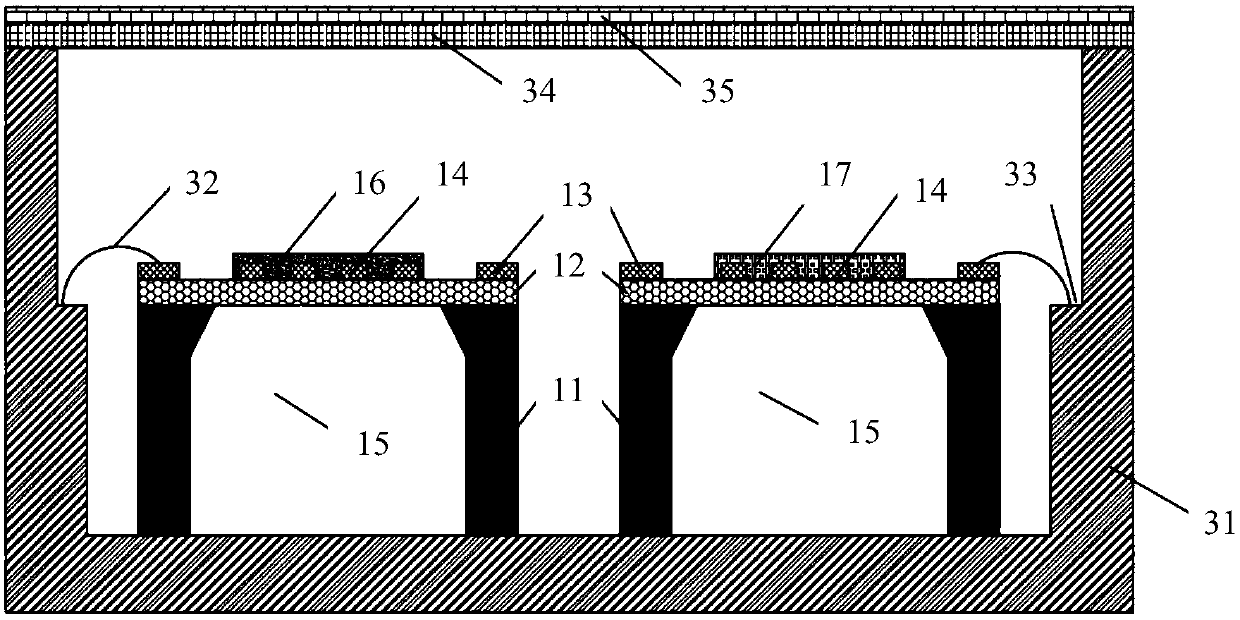
Catalytic combustion gas sensor based on ceramic-based micro-hotplate and preparation method of sensor
A gas sensor, catalytic combustion technology, applied in instruments, scientific instruments, measuring devices, etc., can solve the problems of expensive equipment, high production cost, and reduced power consumption of catalytic combustion gas sensors.
- Summary
- Abstract
- Description
- Claims
- Application Information
AI Technical Summary
Problems solved by technology
Method used
Image
Examples
preparation example Construction
[0138] Based on the above embodiment, another embodiment of the present invention also provides a preparation method for preparing the catalytic combustion gas sensor described in the above embodiment, the preparation method is as follows Figure 8 as shown, Figure 8 A schematic flow diagram of a preparation method provided by an embodiment of the present invention, the preparation method comprising:
[0139] Step S11: providing a silicon substrate, the silicon substrate has a first surface and a second surface opposite to each other; the first surface has a central heating area and a peripheral supporting area.
[0140] For the material and thickness of the silicon substrate, reference may be made to the above description, which will not be repeated here.
[0141] Step S12: forming a film layer of ceramic slurry on the first surface.
[0142] The ceramic slurry is prepared according to the desired target properties of the ceramic membrane. Ceramic slurry can be composed o...
Embodiment 1
[0176] Provide a double-sided polished double-sided oxidized 4-inch monocrystalline silicon wafer with 100 crystal orientation, then ultrasonically clean it with acetone for 15 minutes, then ultrasonically clean it with isopropanol for 5 minutes, then clean it with deionized water for 5 minutes, and blow it with nitrogen Dry; select ceramic powder with appropriate specifications, add organic carrier, configure ceramic slurry, print on the wafer by screen printing, and dry at 120°C for 10 minutes; put the dried wafer into In a muffle furnace, sinter at 1000°C for 30 minutes to obtain a dense and hard ceramic film with a thickness of 10 um, and the surface of the ceramic film is treated by grinding and polishing, so that the surface roughness of the ceramic film is controlled at 0.2 um.
[0177] Print a snake-shaped heating resistor array and a heating electrode array with a length and width of 300um×300um on the ceramic film by screen printing, dry at 120°C for 5min, and sinter ...
Embodiment 2
[0180] Provide a double-sided polished double-sided unoxidized 6-inch monocrystalline silicon wafer with 100 crystal orientation, then ultrasonically clean it with acetone for 10 minutes, then ultrasonically clean it with isopropanol for 10 minutes, then clean it with deionized water for 5 minutes, and clean it with nitrogen gas Blow dry; choose ceramic powder of appropriate specifications, add organic carrier, configure ceramic slurry, use tape casting to make the ceramic slurry form a film on the wafer, and dry at 150 ° C for 10 minutes; dry the The wafer was placed in a muffle furnace and sintered at 1000°C for 30 minutes to obtain a dense and hard ceramic film with a thickness of 20 um. The surface of the ceramic film was treated by grinding and polishing, so that the surface roughness of the ceramic film was controlled at 0.2 um.
[0181] Print a serpentine heating resistor array and heating electrode array with a length and width of 400um×400um on the ceramic film by scre...
PUM
| Property | Measurement | Unit |
|---|---|---|
| Thickness | aaaaa | aaaaa |
| Thickness | aaaaa | aaaaa |
| Resistivity | aaaaa | aaaaa |
Abstract
Description
Claims
Application Information


