Phase-changing material-based adjustable slow light device and fabrication method and application thereof
A phase-change material and device technology, applied in the fields of instruments, optics, nonlinear optics, etc., can solve the problems of limited device modulation band, no modulation space, single modulation method, etc., and achieve wide operating frequency range, various phase change conditions, Effects over a wide frequency range
- Summary
- Abstract
- Description
- Claims
- Application Information
AI Technical Summary
Problems solved by technology
Method used
Image
Examples
Embodiment 1
[0075] This embodiment is used to illustrate the preparation method of the adjustable slow light device of the present invention.
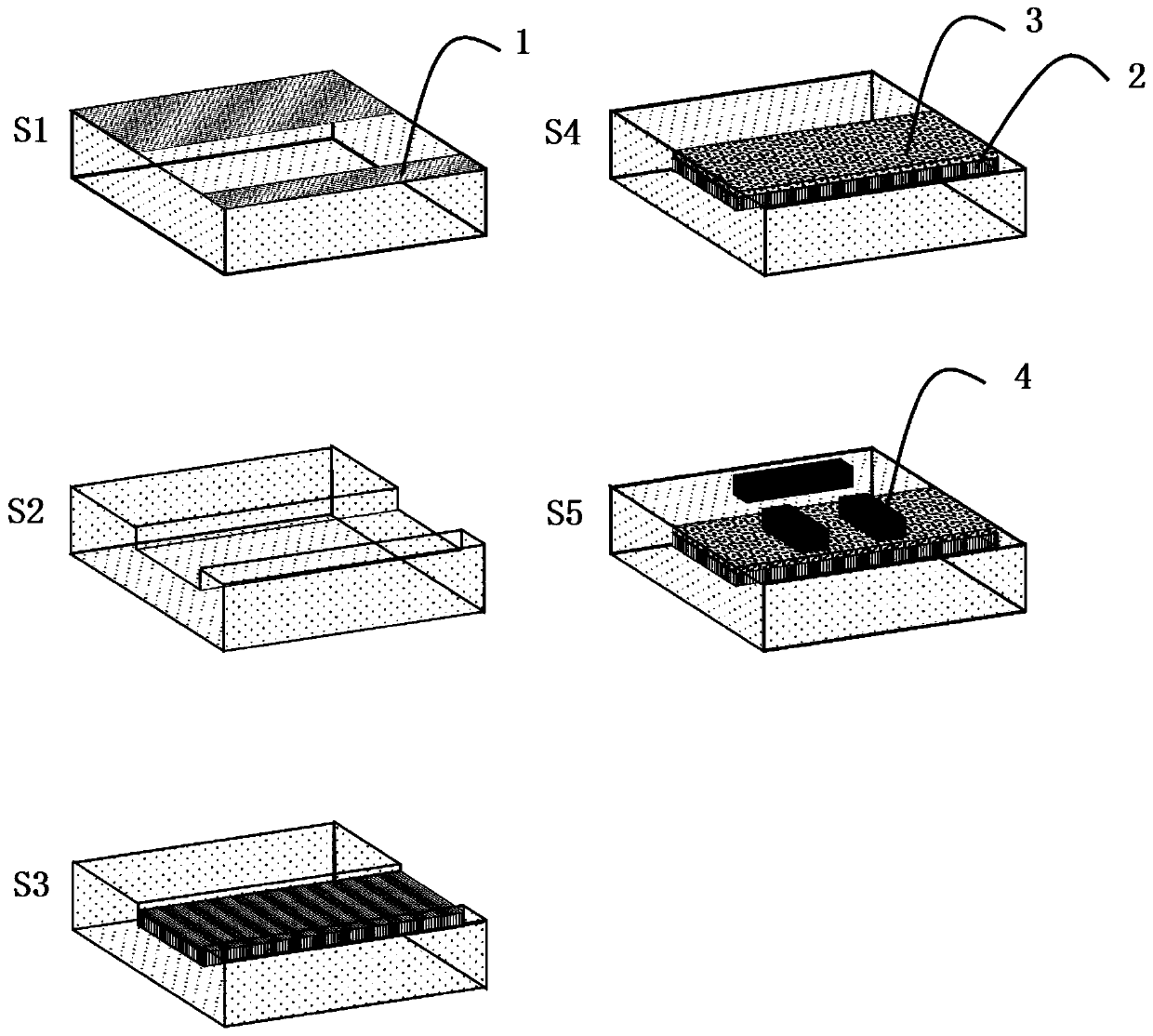
[0076] figure 1 The process flow chart of the adjustable slow light device prepared in Example 1 of the present invention is shown.
[0077] Step S1. Spin-coating photoresist 1 on a clean light-transmitting dielectric substrate, and obtain a periodic strip structure through exposure and other means; the dielectric substrate is a low-loss dielectric that can transmit light in the required response band, including quartz , Silicon wafer, sapphire substrate, etc.
[0078] Step S2. The periodic strip structure described in step S1 is etched into grooves; the depth of the grooves is consistent with the thickness of subsequent film deposition. The appropriate etching method is selected according to the material of the dielectric substrate. The method can be either dry etching technique or physical chemical etching.
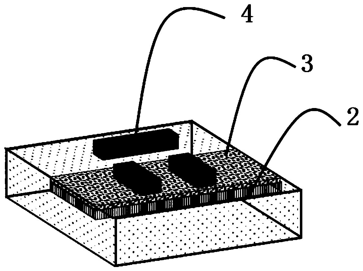
[0079] Step S3. Depositing the phase chang...
Embodiment 2-3
[0097] This embodiment is used to illustrate the preparation method of the adjustable slow light device of the present invention.
[0098] Using the same method as in Example 1, the only difference is that the raw materials are replaced, and the tunable slow light device can also be obtained. The materials and properties are shown in the following table.
[0099] Table 1 Preparation and properties of different tunable slow light devices
[0100]
[0101] The deposition conditions of silicon oxide and aluminum oxide for the dielectric protective layer in the above embodiments are as follows:
[0102] Among them, the deposition of silicon oxide requires a plasma enhanced chemical vapor deposition system (System100 PECVD, Oxford Instruments, UK), the deposition of silicon oxide uses a reactive gas and the ratio is SiH4:N2O:N2=10sccm:327sccm:1000sccm, the deposition temperature is 110℃, and the power 10W, pressure 650mTorr, deposition rate about 2nm / s. The deposition of aluminum oxide re...
PUM
| Property | Measurement | Unit |
|---|---|---|
| width | aaaaa | aaaaa |
| depth | aaaaa | aaaaa |
| thickness | aaaaa | aaaaa |
Abstract
Description
Claims
Application Information


