Organic thin film transistor and preparation method thereof and display device
An organic thin film and transistor technology, applied in the fields of organic thin film transistors and their preparation methods and display devices, can solve the problems of poor mechanical/thermal stability and mismatch of mechanical/thermal stability, etc., to reduce thermal expansion coefficient and avoid transfer failure Complete, improve the effect of electrical contact and service life
- Summary
- Abstract
- Description
- Claims
- Application Information
AI Technical Summary
Problems solved by technology
Method used
Image

Examples
preparation example Construction
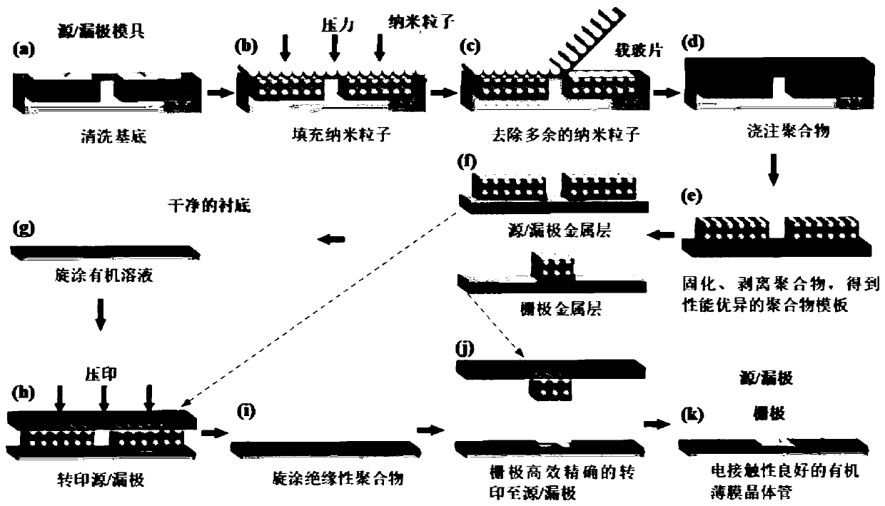
[0035] The invention provides a method for preparing an organic thin film transistor, wherein a sufficient amount of nanoparticles is filled on the surface of a source / drain mold and a grid mold respectively to obtain a source / drain mold and a grid mold filled with nanoparticles; The surface of the source / drain mold and the gate mold with nanoparticles is poured with a polymer solution. After curing, the mold is turned over to transfer the nanoparticles with the polymer to obtain a source / drain template and a gate template; using sputtering technology, the Prepare the source / drain metal layer on the source / drain template, prepare the gate metal layer on the surface of the gate template; transfer the source / drain metal layer to the flexible substrate with the organic semiconductor layer by hot embossing method , to form a flexible substrate for transferring the active / drain metal layer; use spin coating method to prepare an insulating layer on the transferred source / drain metal ...
Embodiment 1
[0052] Embodiment 1 provides a method for preparing an organic thin film transistor, comprising the following steps:
[0053] Step 1. Select a highly doped silicon wafer as a hard substrate, and use etching technology to etch a micron source / drain array structure on a highly doped silicon wafer to obtain a source / drain mold; a micron source / drain array structure The size characteristics are: length × width × depth = 50 × 30 × 25μm;
[0054] Select a highly doped silicon wafer as a hard substrate, and use etching technology to etch a micron grid array structure on a highly doped silicon wafer to obtain a gate mold; the size characteristics of the micron grid array structure are: length × width × depth =12×40×25μm;
[0055] Step 2. Ultrasonic cleaning the source / drain mold or gate mold in step 1 with acetone, ethanol and deionized water in sequence, and drying with nitrogen to make the surface clean;
[0056] Step 3. Fill a sufficient amount of silicon dioxide nanoparticles on...
Embodiment 2
[0069] Embodiment 2 provides a method for preparing an organic thin film transistor, comprising the following steps:
[0070] Step 1. Select a highly doped silicon wafer as a hard substrate, and use etching technology to etch a micron source / drain array structure on a highly doped silicon wafer to obtain a source / drain mold; a micron source / drain array structure The size characteristics are: length × width × depth = 8 × 5 × 1μm;
[0071] Select a highly doped silicon wafer as a hard substrate, and use etching technology to etch a micron grid array structure on a highly doped silicon wafer to obtain a gate mold; the size characteristics of the micron grid array structure are: length × width × depth =3×8×1 μm;
[0072] Step 2. Ultrasonic cleaning the source / drain mold or gate mold in step 1 with acetone, ethanol and deionized water in sequence, and drying with nitrogen to make the surface clean;
[0073] Step 3. Fill a sufficient amount of titanium dioxide nanoparticles on the...
PUM
| Property | Measurement | Unit |
|---|---|---|
| Thickness | aaaaa | aaaaa |
| Young's modulus | aaaaa | aaaaa |
| Thickness | aaaaa | aaaaa |
Abstract
Description
Claims
Application Information
 - Generate Ideas
- Intellectual Property
- Life Sciences
- Materials
- Tech Scout
- Unparalleled Data Quality
- Higher Quality Content
- 60% Fewer Hallucinations
Browse by: Latest US Patents, China's latest patents, Technical Efficacy Thesaurus, Application Domain, Technology Topic, Popular Technical Reports.
© 2025 PatSnap. All rights reserved.Legal|Privacy policy|Modern Slavery Act Transparency Statement|Sitemap|About US| Contact US: help@patsnap.com