A class of blended films based on supramolecular interaction, preparation and preparation method thereof, and applications of blended film in film devices

A thin film and blending technology, which is applied in the manufacture of electrical solid devices, semiconductor devices, semiconductor/solid devices, etc., can solve problems such as ineffective work, high power consumption, and inability to use portable electronic products, achieving chemical stability and Strong chemical modification and improved blendability

Inactive Publication Date: 2020-02-11
SOUTH CHINA UNIV OF TECH
View PDF1 Cites 0 Cited by
  • Summary
  • Abstract
  • Description
  • Claims
  • Application Information

AI Technical Summary

Problems solved by technology

The former cannot work effectively at room temperature due to the high background noise due to the high dark current itself
The latter is too expensive for general commercial use and requires the addition of a power-hung...

Method used


Image

  • A class of blended films based on supramolecular interaction, preparation and preparation method thereof, and applications of blended film in film devices
  • A class of blended films based on supramolecular interaction, preparation and preparation method thereof, and applications of blended film in film devices
  • A class of blended films based on supramolecular interaction, preparation and preparation method thereof, and applications of blended film in film devices

Examples


Embodiment example 1

[0028] Implementation Case 1 Preparation of Supramolecular Interaction Blend Films

[0029] polybenzoselenodiazol-bithienocyclopentadiene alternating copolymer (hereinafter referred to as P1) and the solid of PC71BM were blended according to the mass ratio of 1:1.5, and then o-dichlorobenzene was added to form a solution of 20 mg / ml.

[0030] The solution was dropped on a quartz plate, and the blended film was obtained after natural drying.

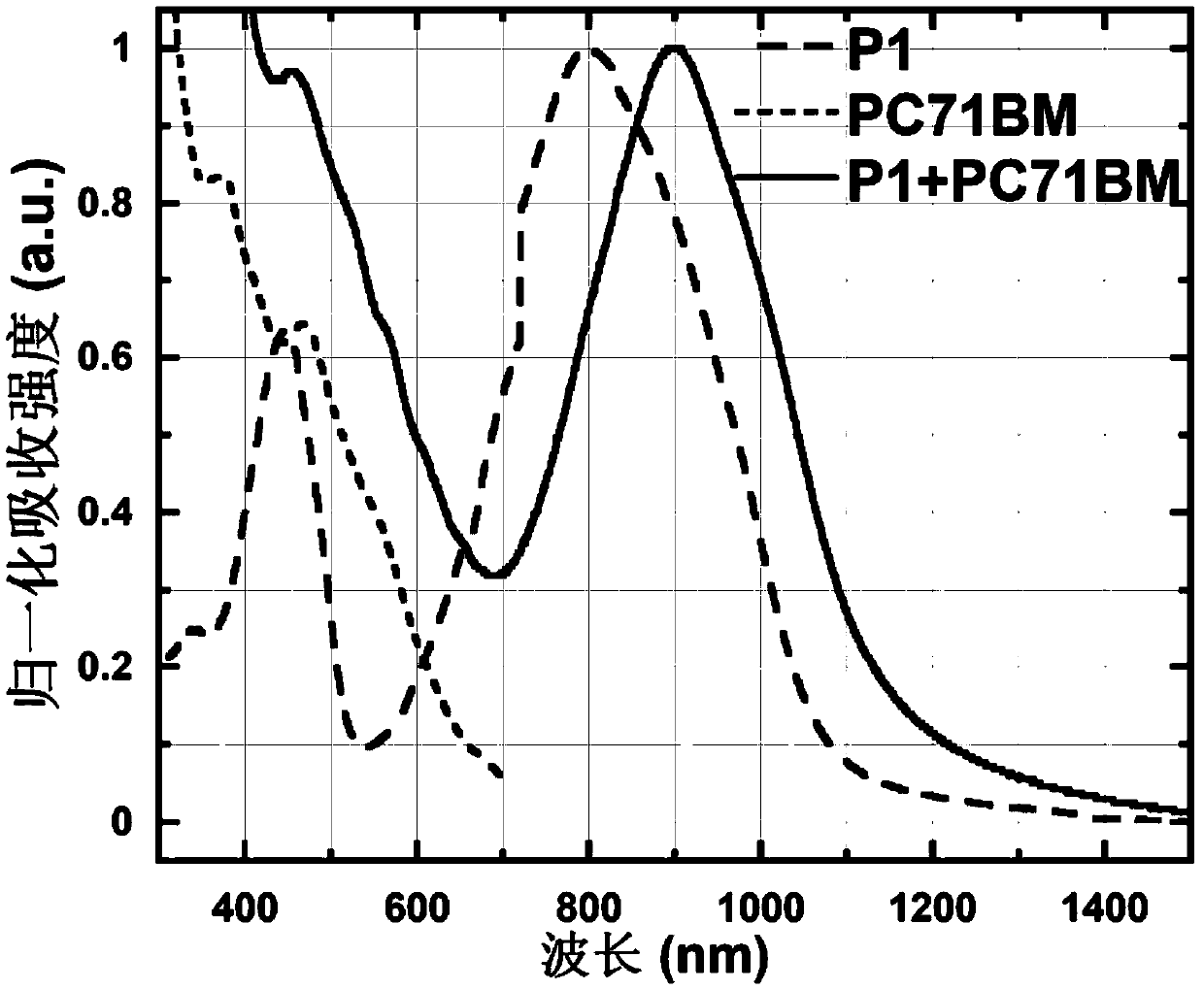
[0031] figure 1 It is the ultraviolet-visible-near-infrared absorption spectrum diagram of P1 and PC71BM blend film. It can be seen from the figure that the absorption spectrum of the blend film is red-shifted than the spectrum of P1 and PC71BM alone.

Embodiment example 2

[0032] Implementation Case 2 Preparation of Supramolecular Interaction Blend Films

[0033] Prepare P1 as a chlorobenzene solution at a concentration of 15 mg / ml; prepare PC71BM as a chlorobenzene solution at a concentration of 30 mg / ml; blend the above two solutions at a mass ratio of 4:3 by volume.

[0034] The solution was dropped on a quartz plate, and the blended film was obtained after natural drying.

Embodiment example 3

[0035] Implementation Case 3 Preparation of Organic Semiconductor Photodetector D1

[0036] The preparation process of the organic semiconductor photodetector of the present embodiment is as follows:

[0037] 1) ITO conductive glass cleaning. Place the ITO glass substrate on the film rack, and use an ultrasonic machine to ultrasonically clean it. The washing liquid is used in the order of acetone, isopropanol, detergent, deionized water and isopropanol, and then placed in an oven at 80 °C to dry.

[0038] 2) ITO is placed in an oxygen plasma etcher, using oxygen plasma (O 2Plasma) carries out the bombardment of 20 minutes, thoroughly removes possible residual organic matter on the surface of the ITO glass substrate;

[0039] 3) Prepare a hole transport layer CH8000 with a thickness of about 40 nm on the surface of the P1asma-treated ITO substrate by solution spin coating, and then thermally anneal at 150 ° C for 15 min;

[0040] 4) Place the annealed ITO substrate in a nit...


PUM


Abstract

The invention discloses applications of supramolecular interaction between a class of compounds containing selenium heterocycle or tellurium heterocycle and fullerene or a fullerene derivative in preparation of film devices, wherein the compound containing selenium heterocycle or tellurium heterocycle has chemical stability, and can form supramolecular interaction with fullerene or fullerene derivative molecules based on the large atom size and the more atom orbits of selenium atoms and tellurium atoms so as to further adjust the optical and electrical properties of the film.

Description

technical field [0001] The invention belongs to the field of organic photoelectric technology, and specifically relates to a blend film based on the interaction of heteroatom compounds and fullerene supramolecules and its application in film devices. Background technique [0002] With the continuous popularization of smart devices, the demand for high-performance and low-cost infrared photoelectric sensors is increasing. Among them, photodetectors and image arrays with short-wave infrared (SWIR, 1-1.4 μm) selectivity have broad application prospects in portable electronics, automotive / residential, automation, human-computer interaction, and artificial intelligence. [0003] Commercial infrared image arrays currently on the market are all based on crystalline silicon wafers. Due to the inherent energy gap of semiconductor silicon, this silicon-based infrared sensor can only be used in the 880-950nm range (that is, the so-called near-infrared NIR band, defined as the 700-1000...

Claims


Application Information

Patent Timeline
IPC IPC(8): C08L65/00C08K3/04C08J5/18H01L51/46
CPCC08J5/18C08J2365/00C08K3/045H10K85/113
Inventor 应磊钟知鸣彭沣黄飞曹镛
Owner SOUTH CHINA UNIV OF TECH
Why Eureka
Try Eureka