A kind of double-layer graphene film LED electrode material and preparation method thereof
A double-layer graphene and graphene film technology, applied in the direction of circuits, electrical components, semiconductor devices, etc., can solve the problems of poor heat dissipation performance, poor electrical conductivity, and poor light transmission performance of electrode materials, and achieve good light transmission characteristics, The effect of low price and excellent thermal conductivity
- Summary
- Abstract
- Description
- Claims
- Application Information
AI Technical Summary
Problems solved by technology
Method used
Image
Examples
Embodiment 1
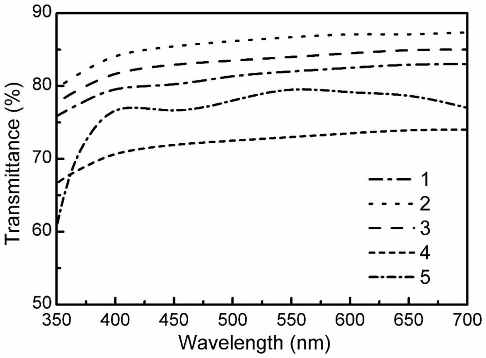
[0026] According to the above technical scheme, this embodiment provides a double-layer graphene film LED electrode material and a preparation method thereof, which specifically includes the following steps:
[0027] Step 1: Put the copper foil substrate with a purity of 99.8% into a vacuum tube furnace, then mix 15sccm of hydrogen, 20sccm of argon, 80sccm of methane and 3sccm of ammonia, and then pass them into the vacuum tube furnace together, and put the tube The furnace was heated to 1100°C for 20 minutes, and the graphene film grown on the surface of the copper foil was taken out after the end.
[0028] Step 2: Spin-coat the PMMA solution onto the graphene film grown on the surface of the copper foil prepared in step 1, specifically fix the graphene film on the glue-spinning machine, make the glue-spinning machine rotate at a speed of 1000r / min, and then apply the PMMA Solution is dripped on above-mentioned Graphene film, utilizes rotation centrifugal force to smear PMMA ...
Embodiment 2
[0032] Embodiment 2 (contrast):
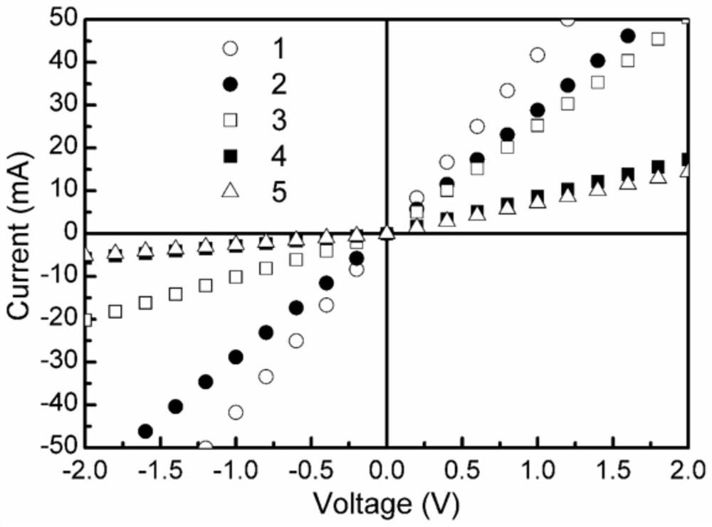
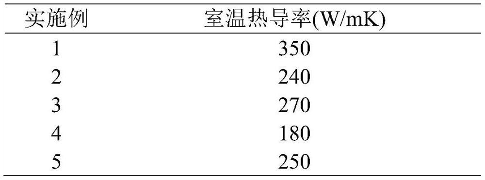
[0033] The preparation method and test are the same as in Example 1, but step 3 is omitted, and molybdenum nitrogen doped graphene film is not added in step 5, and the electrode finally prepared is single-layer graphene rather than double-layer graphene film LED electrode material . It can be seen from Table 1 that its thermal conductivity is 240W / mK, which is significantly lower than the thermal conductivity of 350W / mK of the double-layer graphene film LED electrode material prepared in Example 1. from figure 2 It can be seen that its conductivity is significantly lower than that of Example 1.
Embodiment 3
[0034] Embodiment 3 (contrast):
[0035]The preparation method and test are the same as in Example 1, but step 4 is omitted, and no iridium-silver-nitrogen-doped graphene film is added in step 5, and the finally prepared electrode is single-layer graphene instead of double-layer graphene. It can be seen from Table 1 that its thermal conductivity is 270W / mK, which is significantly lower than the thermal conductivity of 350W / mK of the double-layer graphene film LED electrode material prepared in Example 1. from figure 2 It can be seen that its conductivity is significantly lower than that of Example 1.
PUM
 Abstract
Description
Claims
Application Information


