P-type local back surface field passivation double-sided solar cell and preparation process thereof

A technology of partial back surface field and double-sided solar cells, which is applied in the field of solar cells to achieve the effects of reducing floor space, saving silicon substrate materials, and reducing series resistance

Pending Publication Date: 2020-02-21
TONGWEI SOLAR ENERGY (CHENGDU) CO LID
View PDF0 Cites 9 Cited by
  • Summary
  • Abstract
  • Description
  • Claims
  • Application Information

AI Technical Summary

Problems solved by technology

[0005] The purpose of the present invention is: in order to solve the existing technical problems, the present invention provides a p-type local back surface field-passivated double-sided solar cell and its preparation process

Method used


Image

  • P-type local back surface field passivation double-sided solar cell and preparation process thereof
  • P-type local back surface field passivation double-sided solar cell and preparation process thereof

Examples


Embodiment 1

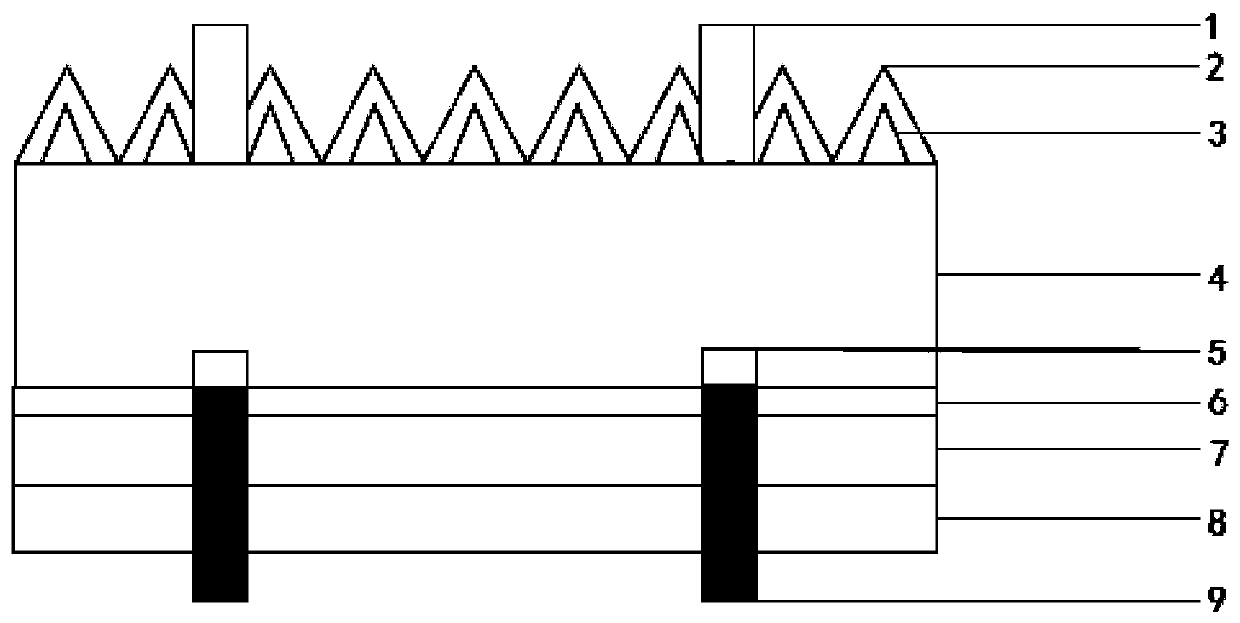
[0035] Such as figure 1 As shown, this embodiment provides a p-type partial back surface field passivation double-sided solar cell, including a p-type silicon substrate 4, and the bottom of the p-type silicon substrate 4 is provided with a silicon oxide passivation layer 6, An aluminum oxide passivation layer 7 and a silicon nitride antireflection layer 8 on the back side, a number of boron source doped layers 5 are embedded at the bottom of the p-type silicon substrate 4, and the bottom of the boron source doped layer 5 is connected with a passivation layer penetrating through silicon oxide at the same time. Layer 6, aluminum oxide passivation layer 7 and backside metal electrode layer 9 of silicon nitride antireflection layer 8.

[0036] A number of boron source doped layers 5 are embedded at the bottom of the p-type silicon substrate 4, thereby forming a back field high-low junction structure, which improves the open circuit voltage of the back cell of the double-sided sola...

Embodiment 2

[0044] Example 2

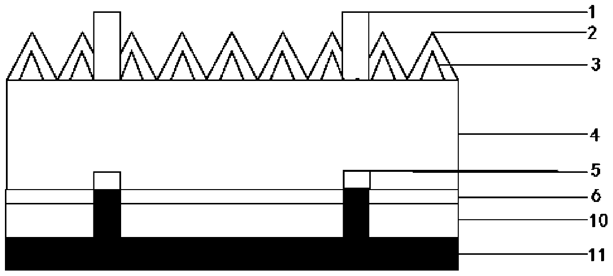
[0045] Such as figure 2 As shown, the present embodiment provides a p-type local back surface field passivation single-sided solar cell, comprising a p-type silicon substrate 4, and the bottom of the n-type silicon substrate is provided with a silicon oxide passivation layer 6 and this The bottom of the n-type silicon substrate is embedded with a number of boron source doped layers 5, and the bottom of the phosphorus source doped layer 3 is connected with a silicon oxide passivation layer 6 and an intrinsic amorphous silicon layer 10. Aluminum back field layer 11, and the aluminum back field layer 11 extends out to cover the lower surface of the intrinsic amorphous silicon layer 10, and the top of the n-type silicon substrate is provided with a phosphorus source doped layer 3 and a front silicon nitride in sequence from bottom to top The anti-reflection layer 2 and the phosphorus source doped layer 3 are provided with a plurality of front metal electrode l...

Embodiment 3

[0047] Such as figure 1 As shown, this embodiment provides a preparation process for a p-type local back surface field-passivated double-sided solar cell, including the following steps:

[0048] S1: select a p-type silicon substrate 4, clean the p-type silicon substrate 4, and perform surface polishing;

[0049] S2: performing low-pressure thermal diffusion on the upper surface of the p-type silicon substrate 4 to prepare the phosphorus source doped layer 3;

[0050] S3: performing ozone oxidation on the lower surface of the p-type silicon substrate 4 to grow a silicon oxide passivation layer 6;

[0051] S4: preparing a front silicon nitride anti-reflection layer 2 on the upper surface of the phosphorus source doped layer 3;

[0052] S5: preparing an aluminum oxide passivation layer 7 on the lower surface of the silicon oxide passivation layer 6;

[0053] S6: preparing a silicon nitride anti-reflection layer 8 on the lower surface of the aluminum oxide passivation layer 7; ...


PUM

PropertyMeasurementUnit
thicknessaaaaaaaaaa
thicknessaaaaaaaaaa
thicknessaaaaaaaaaa

Abstract

The invention discloses a p-type local back surface field passivation double-sided solar cell and a preparation process thereof, and relates to the technical field of solar cells. The solar cell comprises a p-type silicon substrate, wherein the bottom of the p-type silicon substrate is provided with a silicon oxide passivation layer, an aluminum oxide passivation layer and a back silicon nitride antireflection layer from top to bottom, the bottom of the p-type silicon substrate is embedded with a plurality of strips of a boron source doped layer, and the bottom of the boron source doping layeris connected with a back metal electrode layer which simultaneously penetrates through the silicon oxide passivation layer, the aluminum oxide passivation layer and the back silicon nitride antireflection layer. During the preparation, a plurality of local slots are formed in the lower surface of the back silicon nitride antireflection layer by using laser, the local slots are formed to the bottom of the p-type silicon substrate, the slotted area is printed with boron source slurry to form a high-low junction structure, the open-circuit voltage of the back cell of the double-sided solar cellis improved, the slotted boron source slurry heavily-doped area is in contact with a metal electrode to form ohmic contact, the series resistance is reduced, the filling factor is improved, and the double-sided rate of the cell is improved under the condition of not reducing the front efficiency.

Description

technical field [0001] The invention relates to the technical field of solar cells, in particular to a p-type local back surface field-passivated double-sided solar cell and a preparation process thereof. Background technique [0002] In recent years, the vigorous development of renewable energy has been increasing day by day. The more popular renewable energy fields include solar energy, wind energy, and tidal energy. Compared with traditional energy sources, solar energy has the characteristics of simple utilization, safety, and no pollution, and has become the focus of research in the field of renewable new energy. The basic principle of solar cell power generation is the photovoltaic effect. Solar cells are new energy devices that convert sunlight into electrical energy. With the increase in the application of solar power generation, new policies and other preferential issues, the cost of photovoltaic power generation needs to be greatly reduced. The cost reduction of p...

Claims


Application Information

Patent Timeline
Patent Type & Authority Applications(China)
IPC IPC(8): H01L31/0216H01L31/0224H01L31/0288H01L31/0352H01L31/068H01L31/18
CPCH01L31/02167H01L31/02168H01L31/0684H01L31/1804H01L31/1868H01L31/035281H01L31/0288H01L31/022441H01L31/022425H01L31/022433H01L31/02366
Inventor 王璞谢毅张鹏眭山
Owner TONGWEI SOLAR ENERGY (CHENGDU) CO LID
Why Eureka
Try Eureka